
A fully-controlled rectifier circuit contains only controlled-rectifiers, whereas a semi-controlled rectifier circuit is made up of both controlled and uncontrolled rectifiers. Due to presence of diodes, free-wheeling operation takes place without allowing the bridge output voltage to become negative. In a semi-controlled rectifier, control is effected only for positve output voltage, and no control is possible when its output voltage tends to become negative since it is clamped at zero volt. This page describes the operation of a single-phase half-controlled rectifier.
A semi-controlled full-wave bridge rectifier can be configured in a few ways. They are shown below.
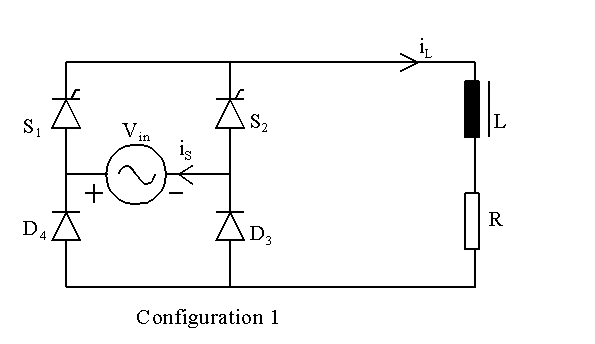
The circuit in Configuration 1 contains two SCRs and two
diodes. When source Vin is positive, SCR S1 can be
triggered at a firing angle called a and then
current flows out of the source through SCR S1 first, then through
the load and returns via diode D3. If

then SCR S1 and diode D3 conduct during
a < wt < p.
When p < wt < 2p,
Vin is negative and SCR S2 is normally triggered
when wt = p + a.
During p < wt < (p
+ a) , the output of the bridge circuit would
have been negative if we had used a fully-controlled bridge rectifer and
if the current flow was continuous. But here we have two diodes D3
and D4 instead of two SCRs. When the output of the bridge tends
to becomes negative just after wt exceeds p,
diode D4 tends to get forward-biased and it starts conducting.
Then diode D3 is reverse-biased and it stops conducting. During
p < wt < (p
+ a) , the devices in conduction are SCR S1
and diode D4 and the output of the bridge is clamped at zero,
assuming that the on-state drops across devices in conduction is zero.
During ( p + a) < wt < 2p
, the devices in conduction are SCR S2 and diode D4.
SCR S2 and diode D3 would conduct during 0 < wt
< a .
The circuit in configuration 1 has SCRs as the devices in the top-half and diodes as the devices in the bottom-half. Instead, it it is possible to use SCRs as the devices in the bottom-half and diodes as the devices in the top-half.
It is also possible to build a semi-controlled full-wave bridge rectifier as shown by the circuit in configuration 2.

The behaviour of the circuit is the same as described
earlier. In this circuit, SCR S1 and diode D3 conduct
during a < wt < p
. During p < wt < (p
+ a) , the devices in conduction are diodes
D3 and D4 and the output of the bridge is clamped
at zero. During (p + a)
< wt < 2p , the devices in conduction
are SCR S2 and diode D4. Diodes D3 and
D4 would conduct during 0 < wt < a
.
Yet another configuration is available for semi-controlled bridge rectifier, as shown by the circuit in configuration 3.

In this circuit, SCRs S1 and S3 conduct
during a < wt < p.
During p < wt < (p
+ a) , the device in conduction is diode D and
the output of the bridge is clamped at zero. During (p
+ a) < wt < 2p
, the devices in conduction are SCRs S2 and S4. Diode
D would conduct during 0 < wt < a .
The aim of analysis is to obtain the following values:
1. The average output voltage of the bridge as a function of firing angle.
2. The rms output voltage of the bridge as a function of firing angle.
3. The ripple factor of output voltage of the bridge as a function of firing angle.
4. The rms line current as a function of firing angle and the ratio wL/R.
5. The fundamental rms line current as a function of firing angle and the ratio wL/R.
6. The THD in line current as a function of firing angle and the ratio wL/R.
The Average Output Voltage


The ripple factor is defined then as

Next it is shown how the line current is to be analysed.
An expression for load current over half-a-cycle can be obtained first.
The load current during a < wt < p
can be defined as follows.

where

From the expression for load current,

The load current during p <
wt < (p + a) can
be defined as follows.

When the load current is repetitive, we have that

That is,

and

Hence we obtain that

Once A is known, the total rms value of line current and
the rms value of its fundamental component can be estimated.
Let

and

Then the rms line current given t and a is obtained as
follows.

To obtain the rms value of the fundamental component
of the line current, we obtain the trigonometric Fourier series coefficients
of the fundamental component. The line current has half-wave symmetry and
hence these coefficients are obtained as follows.

Then

We obtain the rms value of fundamental component as:
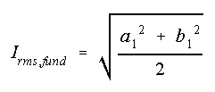
Total harmonic distortion in line current is then
The applet shown below simulates this circuit. The parameters to be keyed-in are the ratio of load reactance to load resistance and the firing angle in degrees.
The semi-controlled bridge rectifier that has been simulated has four SCRs and a single free-wheeling diode. The program is presented below.
* Full-wave Bridge Rectifier with a resistive load
VIN 1 0 SIN(0 340V 50Hz)
XT1 1 2 5 2 SCR
XT2 0 2 6 2 SCR
XT3 4 0 7 0 SCR
XT4 4 1 8 1 SCR
VP1 5 2 PULSE(0 10 1667U 1N 1N 100U 20M)
VP2 6 2 PULSE(0 10 11667U 1N 1N 100U 20M)
VP3 7 0 PULSE(0 10 1667U 1N 1N 100U 20M)
VP4 8 1 PULSE(0 10 11667U 1N 1N 100U 20M)
D1 4 2 DNAME
L1 2 3 31.8M
R1 3 4 10
R2 1 0 1MEG
R3 2 0 1MEG
R4 4 0 1MEG
.MODEL DNAME D(IS=10N N=1 BV=1200 IBV=10E-3 VJ=0.6)

* Subcircuit for SCR
.SUBCKT SCR 101 102 103 102
S1 101 105 106 102 SMOD
RG 103 104 50
VX 104 102 DC 0
VY 105 107 DC 0
DT 107 102 DMOD
RT 106 102 1
CT 106 102 10U
F1 102 106 POLY(2) VX VY 0 50 11
.MODEL SMOD VSWITCH(RON=0.0105 ROFF=10E+5 VON=0.5 VOFF=0)
.MODEL DMOD D((IS=2.2E-15 BV=1200 TT=0 CJO=0)
.ENDS SCR
.TRAN 10US 60.0MS 0.0MS 10US
.FOUR 50 V(2,4) I(VIN)
.PROBE
.OPTIONS(ABSTOL=1N RELTOL=.01 VNTOL=1MV)
.END
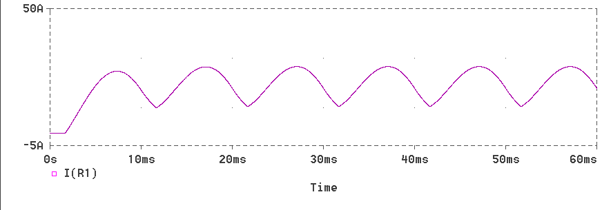
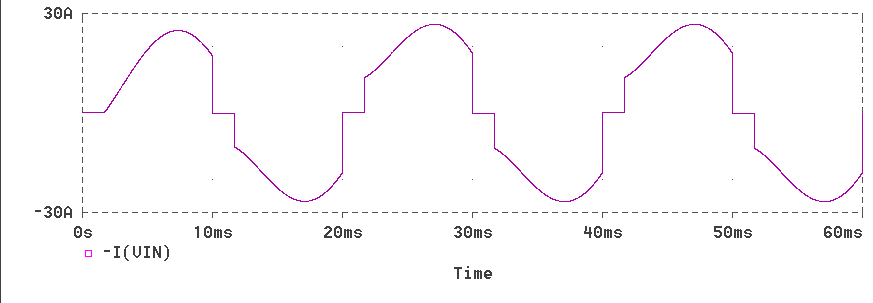
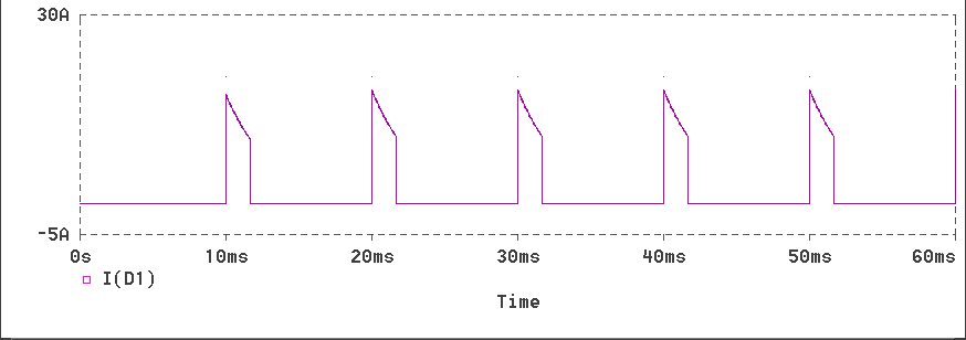
The waveforms obtained are displayed.
The waveform of bridge output voltage

This page has described how a semi-controlled bridge rectifier operates. The next chapter is on fully-controlled three-phase bridge recitifier circuit.