
INTRODUCTION
BASIC CIRCUIT OPERATION
DISCONTINUOUS OPERATION
CONTROL BY PULSE-WIDTH MODULATION
CLOSED-LOOP CONTROL
MICRO-CONTROLLER IMPLEMENTATION
IMPLEMENTATION USING A MULTIPLIER
SUMMARY
A buck converter or step-down switch mode power supply can also be called a switch mode regulator. Popularity of a switch mode regulator is due to its fairly high efficiency and compact size and a switch mode regulator is used in place of a linear voltage regulator at relatively high output. Linear voltage regulators tend to be inefficient. Since the power devices used in linear regulators have to dissipate a fairly large amount of power, they have to be adequately cooled, by mounting them on heatsinks and the heat is transferred from the heatsinks to the surrounding air either by natural convection or by forced-air cooling. Heatsinks and provision for cooling makes the regulator bulky and large. In applications where size and efficiency are critical, linear voltage regulators cannot be used.
A switch mode regulator overcomes the drawbacks of linear regulators. Switched power supplies are more efficient and they tend to have an efficiency of 80% or more. They can be packaged in a fraction of the size of linear regulators. Unlike linear regulators, switched power supplies can step up or step down the input voltage.
The buck converter is introduced using the evolutionary approach. Let us consider the circuit in Fig. 1, containing a single pole double-throw switch.

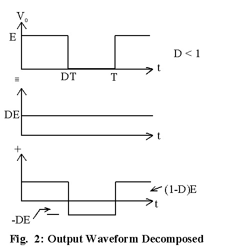
For the circuit in Fig. 1, the output voltage equals the input voltage when the switch is in position A and it is zero when the switch is in position B. By varying the duration for which the switch is in position A and B, it can be seen that the average output voltage can be varied, but the output voltage is not pure dc. The output voltage contains an average voltage with a square-voltage superimposed on it, as shown in Fig. 2.. Usually the desired outcome is a dc voltage without any noticeable ripple content and the circuit in Fig. 1 is to be modified.
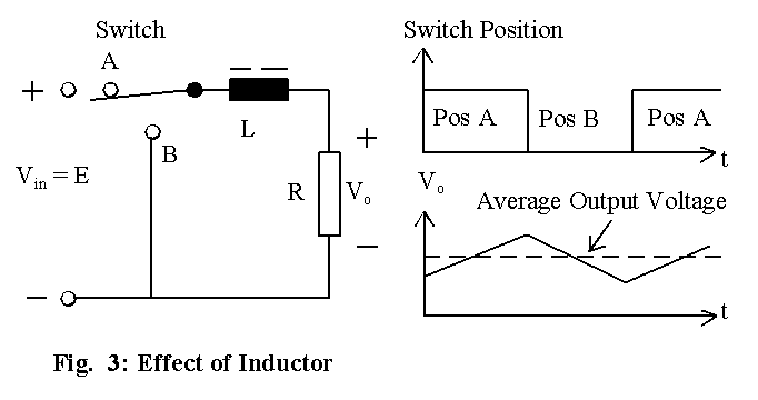
The circuit in Fig. 1 can be modified as shown in Fig. 3 by adding an inductor in series with the load resistor. An inductor reduces ripple in current passing through it and the output voltage would contain less ripple content since the current through the load resistor is the same as that of the inductor. When the switch is in position A, the current through the inductor increases and the energy stored in the inductor increases. When the switch is in position B, the inductor acts as a source and maintains the current through the load resistor. During this period, the energy stored in the inductor decreases and its current falls. It is important to note that there is continuous conduction through the load for this circuit. If the time constant due to the inductor and load resistor is relatively large compared with the period for which the switch is in position A or B, then the rise and fall of current through inductor is more or less linear, as shown in Fig. 3.
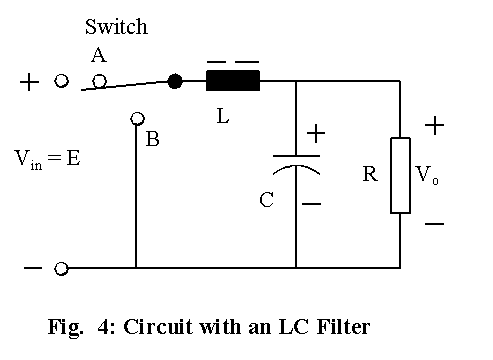
The next step in evolutionary development of the buck converter is to add a capacitor across the load resistor and this circuit is shown in Fig. 4. A capacitor reduces the ripple content in voltage across it, whereas an inductor smoothes the current passing through it. The combined action of LC filter reduces the ripple in output to a very low level.
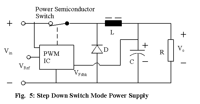
The circuit in Fig. 4 contains a single-pole double-throw switch. It is a difficult configuration to realize using power semiconductor devices. On the other hand, an understanding of the circuit in Fig. 4 leads to a realizable and simple configuration. When the switch is in position A, the current through the inductor and it decreases when the switch is in position B. It is possible to have a power semiconductor switch to correspond to the switch in position A. When switch is in position B, the inductor current free-wheels through it and hence a diode can be used for free-wheeling operation. Then only the power semiconductor switch needs to be controlled, and in practice, a pulse-width modulating IC is used. The circuit that results is shown in Fig. 5.
Generally any basic switched power supply consists of five standard components:
An inductor is used in a filter to reduce the ripple in current. This reduction occurs because current through the inductor cannot change suddenly. When the current through an inductor tends to fall, the inductor tends to maintain the current by acting as a source. Inductors used in switched supplies are usually wound on toroidal cores, often made of ferrite or powdered iron core with distributed air-gap to minimize core losses at high frequencies.
A capacitor is used in a filter to reduce ripple in voltage. Since switched power regulators are usually used in high current, high-performance power supplies, the capacitor should be chosen for minimum loss. Loss in a capacitor occurs because of its internal series resistance and inductance. Capacitors for switched regulators are chosen on the basis of effective series resistance (ESR). Solid tantalum capacitors are the best in this respect. For very high performance power supplies, sometimes it is necessary to parallel capacitors to get a low enough effective series resistance.
The diode used in a switched regulator is usually referred to as free-wheeling diode or sometimes as a catch diode. The purpose of this diode is not to rectify, but to direct current flow in the circuit and to ensure that there is always a path for the current to flow into the inductor. It is also necessary that this diode should be able to turn off relatively fast. Diodes known as the fast recovery diodes are used in these applications.
Most of the switched supplies needs a minimum load, in order to ensure that the inductor carries current always. If the current flow through the inductor is not continuous, regulation may become poorer.
The buck converter or SMPS can be controlled in two ways, known as :
When control by frequency modulation is to be achieved, the ON period of the power semiconductor switch is kept constant and the frequency of operation is varied to effect voltage regulation. Design of LC filter is not easy in such a case.
If a micro-controller is used instead of a specific PWM IC, it is possible to switch from one mode of control to the other depending on the load conditions.
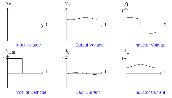
The operation of the buck converter is explained first. This circuit can operate in any of the three states as explained below. The first state corresponds to the case when the switch is ON. In this state, the current through the inductor rises, as the source voltage would be greater than the output voltage, whereas the capacitor current may be in either direction, depending on the inductor current and the load current. When the inductor current rises, the energy stored in it increases. During this state, the inductor acquires energy.
When the switch is closed, the elements carrying current
are shown in red colour in Fig. 6, whereas the diode is in gray, indicting
that it is in the off state. In Fig. 6(a), the capacitor is getting charged,
whereas it is discharging in Fig. 6(b).
FIG. 6(a): 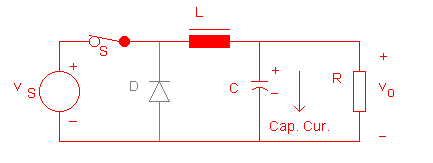
FIG. 6(b): 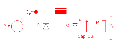
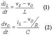
The equations that govern the operation of the circuit in the first state are shown below.
The second state relates to the condition when the switch is off and the diode is ON. In this state, the inductor current free-wheels through the diode and the inductor supplies energy to the RC network at the output. The energy stored in the inductor falls in this state. In this state, the inductor discharges its energy and the capacitor current may be in either direction, depending on the inductor current and the load current Figure 7 illustrates the second state.
FIG. 7(a): 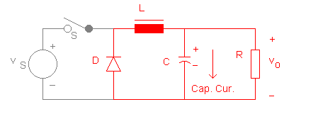
FIG. 7(b): 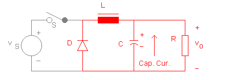
The equations that govern the operation of the circuit in the second state are shown below.

When the switch is open, the inductor discharges its energy. When it has discharged all its energy, its current falls to zero and tends to reverse, but the diode blocks conduction in the reverse direction. In the third state, both the diode and the switch are OFF and Fig.8 illustrates the third state. During this state, the capacitor discharges its energy and the inductor is at rest, with no energy stored in it. The inductor does not acquire energy or discharge energy in this state.
FIG. 8: 
The equation that governs the operation of the circuit in the third state is shown below.

When the circuit receives a periodic signal, the response of the circuit also becomes periodic. Here it is assumed that the source voltage remains constant with no ripple, and the frequency of operation is kept fixed with a fixed duty cycle. If the RC time constant due to the load resistor and the filter capacitor is very large compared to the cycle period of the switching frequency, the output voltage is more or less constant, with no noticeable ripple. When both the input voltage and the output voltage are constant, the current through the inductor rises linearly when the switch is ON and it falls linearly when the switch is OFF. Under this condition, the current through the capacitor also varies linearly when it is getting charged or discharged.
The responses obtained for a particular set of parameters are displayed in Fig. 9. The values of parameters used are:
Source voltage = 100 V dc,
Switching frequency = 20 kHz,
L = 500 mH,
C = 500 mF,
R = 10 W,
and
duty cycle = 0.5.
The value of 1 in a voltage plot in Fig. 9 corresponds
to 100 V and the value of 1 in a current plot corresponds to 10 A. Figure
9 displays the responses over one cycle.

Fig.9: Periodic Response with a dc voltage Input
An expression for the average output voltage can be obtained as follows. It is assumed that there is continuous conduction in the inductor. Given that the cycle period is T, the ON-period is DT, and the source voltage is E,
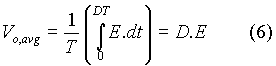
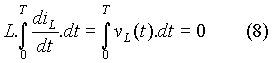
In eqn. (6), D stands for the duty cycle. The same expression for output voltage can be obtained in another way. When the responses in the circuit are periodic, the inductor current is the same at the beginning and end of a cycle. That is,
![]()
Equation (7) can be expressed as follows:
When the switch is ON, vL(t) = E - Vo,avg and when the diode is conducting,
vL(t) = - Vo,avg. Therefore


On evaluation,

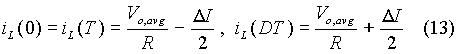
The change in inductor current when the switch is On can be determined as follows. Let the change in inductor current be DI, as shown in Fig. 10. In this figure, the change in output voltage has been exaggerated for sake of clarity. When the switch is ON, the voltage across the inductor can be expressed as:

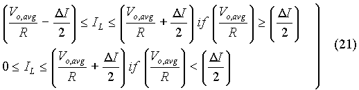
When the output voltage remains steady at Vo,avg, the inductor current linearly during the ON period of the switch. Then

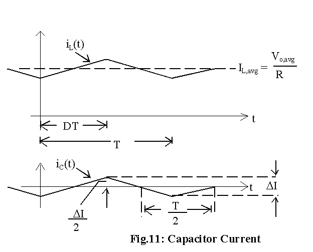
During the ON-period, the inductor current rises from (Vo,avg/R - DI/2) to (Vo,avg/R + DI/2). That is,
The capacitor current iC is expressed as follows:
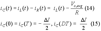
Now an assumption is made to find out the change in output voltage. It is assumed that the capacitor gets charged for half of the cycle period and gets discharged during the other half , as shown in Fig. 11. Since the current through the capacitor varies linearly, the average charging current is half of its peak value of the triangular waveform. The peak value of its triangular waveform is shown to be DI/2. Hence
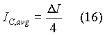
If a periodic signal has zero dc value over its cycle period, its average is defined based only on its positive part and hence the average capacitor current is obtained as shown above. For a capacitor
![]()
Based on the average charging current and half of the cycle period as the charging period, we get the change in output voltage DV as:
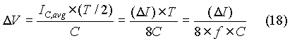
Using equation (12), the above equation can be expressed as:

Assuming that the ripple in output voltage is sinusoidal, the rms value of ripple content in output voltage is:
Note that the variation in output voltage is not shown to be sinusoidal in Fig. 10.. Even though the variation appears to be triangular, equation (20) gives a better approximation of the rms value of ripple content in output voltage.
Given that source voltage = 100 V dc, switching frequency = 20 kHz, L = 500 mH, C = 500 mF, R = 10 W, and duty cycle = 0.5, the results obtained are:
Vo,avg = 50 V,
DI = 2.5 A,
DV = 31.25 mV, and
Vrms,ripple = 11.05 mV.
In order that the capacitor current and the inductor current vary linearly, it is necessary that the RC time constant should be relatively large, equal to about four or five times the cycle period. When the RC time constant is much smaller than the cycle period, the responses obtained are not linear. To illustrate, Fig. 12 displays another set of responses. The only change is that a 1 mF capacitor is used in place of the 500 mF capacitor.
When the RC time constant is small, the output voltage contains noticeable ripple. In addition, the ripple in output voltage appears to be sinusoidal, justifying the equation used for finding out the rms value of the ripple content in output voltage. Another aspect can be noticed in Fig. 12. It is that the ripple in output voltage goes through its negative half-cycle when the switch is ON. When this circuit is to be controlled by negative feedback, the feedback at the ripple frequency would become positive and closed-loop control effected without taking this aspect into account would produce a larger ripple in the output.
Transient Response

Fig. 13 Transient Response
Let us assume that the output voltage is zero and that there is no current through the inductor at start. If the source voltage is connected suddenly and the switch is turned ON and OFF at a fixed frequency with a preset duty cycle, the transient response of the circuit lasts for several cycles before it settles down to periodic response. The inrush current through the inductor is quite high, several times the maximum current that can flow under settled conditions. The transient response obtained over the first 10 ms with source voltage = 100 V dc, switching frequency = 20 kHz, L = 500 mH, C = 500 mF, R = 10 W, and duty cycle = 0.5, is shown in Fig. 13 . Even after 200 cycles, the response is still in the transient state.
Effect of ripple in input voltage
Usually the input to an SMPS happens to be an unregulated dc voltage provided by a rectifier-filter circuit. Such a filter contains significant ripple content at double the line frequency. The first applet in this page illustrates the response obtained when the input voltage contains ripple. In this program, the ripple frequency, the peak-to-peak ripple and the source voltage can be set. If the source voltage = 100 V, peak-to-peak ripple voltage = 20 V, and the ripple frequency = 100 Hz, then the input voltage falls from 110 V to 90 V in the first 7.5 ms and rises from 90 V to 110 V in the remaining 25% of the input cycle period. The input voltage falls linearly in the initially for 75% of the cycle period from (E + Vrip,pk-to-pk/2) to (E - Vrip,pk-to-pk/2) and then rises linearly during the remainder of the input cycle period.
When the input voltage varies cyclically, the response of the circuit is periodic over its input cycle period and it is not periodic not over the period corresponding the switching frequency. In addition, there is significant overshoot in the inductor current when the input voltage is rising linearly. It can also be seen that the output voltage has nearly the same waveform as the input voltage, which is only to be expected. Since the duty cycle is kept fixed, the output voltage would tend to rise as the input voltage rises. The response obtained with a peak-to-peak ripple voltage of 20 V at 100 Hz is shown in Fig. 14. It becomes clear from the response that closed-loop control is necessary to maintain the output voltage when the input voltage has some ripple content. The closed-loop control circuit has to be designed with care, since the duty cycle has to be continually varied to maintain the output voltage at its set value.
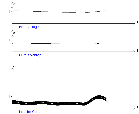
Fig. 14: Periodic Response over One Input Cycle Period
Effect of Step Change in Load
When there is a step change in load, the circuit goes through transient response before it settles back to periodic response. Here the circuit is allowed to be a settled state with a load resistance of 10 W. Then the load resistance is changed to 5 W and the transient response that is obtained is presented in Fig. 15. In Fig. 15, '1' on the axis for corresponds to 10 A.
When the load resistor was 10 W, the load current would have been 5 A given that the duty cycle is 0.5 and the input voltage is 100 V. It can be seen that after the step change in load resistor, the output voltage dips first and then recovers. If the change is in the other direction from 5 W to 10 W, the output voltage rises first before falling back, as shown in Fig. 16. For this figure, '1' on the axis for corresponds to 20 A.
Effective closed-loop control would reduce the transients. The under-damped nature of inductor current response can be improved.
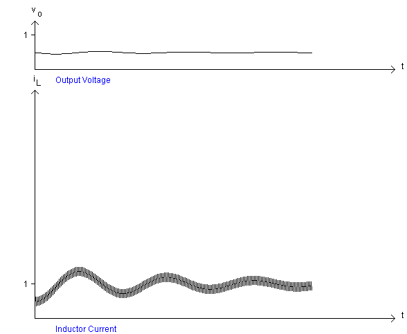
Fig. 15: Effect of Step Load Change: Increase in Load
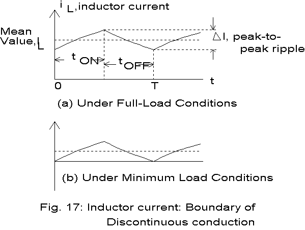
When the load resistor becomes high, the buck converter circuit operates in the discontinuous mode. The inductor current falls to zero when the switch is open and remains at zero till the switch becomes ON in the next cycle. Such a mode is the desirable mode of operation when variable frequency of operation is employed for voltage control. Additionally, discontinuous operation puts less stress on the diode and the circuit operates well. This aspect will be explained later.
The effect of load resistance on the inductor current is shown in Fig. 17. Given that the conduction is continuous, the average load current is Vo,avg/R. As the load resistance increases, the average load current decreases, but on the other hand, the change in inductor current as defined by equation (12) remains constant. As indicated by equation (13), the inductor current remains within the range specified below.
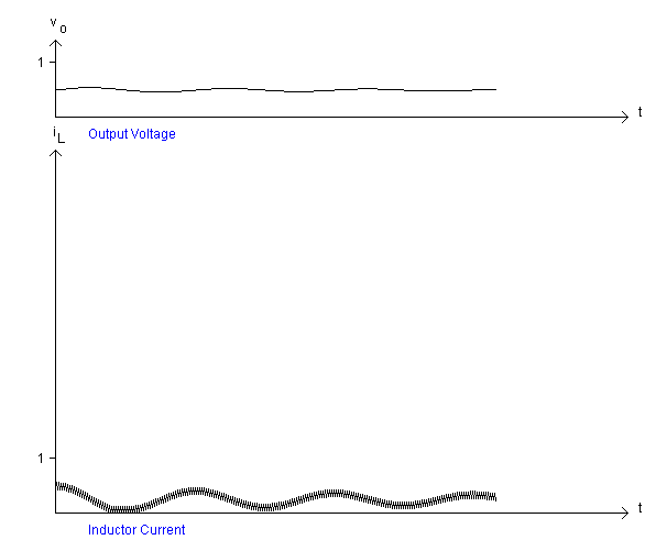
Fig. 16: Effect of Step Load Change: Reduction in Load
When the inductor current is continuous, the value of Vo,avg is as defined by equation (10) and it is not so if the conduction is discontinuous. After substituting for DI from equation (12), we get that
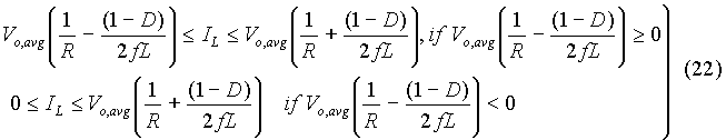
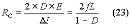
Hence a critical resistance, say RC can be defined that makes the circuit operate at boundary of continuous conduction, a situation illustrated in Fig. 17. When the load resistance is higher than the conduction in inductor is discontinuous and it is continuous if the load resistance is less than RC .
It can be seen from equation that at the boundary of continuous and discontinuous conduction,
Discontinuous operation is illustrated in Fig. 18. In
Fig. 18, the duty cycle for the switch is defined to D1, and
the duty cycle for the diode is defined to D2. It means that
in each cycle, the switch conducts for a time interval equal to D1T
and the diode conducts for a time interval equal to D2T, where
T is the cycle period. It can be seen that for discontinuous conduction
![]()
At the boundary of continuous and discontinuous conduction, (D1 + D2) = 1. Given that the discontinuous, there is no current in the inductor for a time interval equal to (1 - D1 -D2)T.
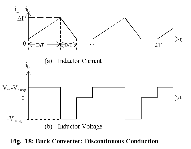
The average load current is the average of the inductor current in Fig. 18. From Fig. 18,


Substituting for DI from equation (24), we get that

Solving for D2,
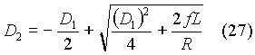
When R > RC, D2 can be obtained from equation (27), assuming that D1, f and L are known. Since the average of the inductor voltage over a cycle is zero, we obtain from Fig. 18 that,
![]()
Then

Substituting for D2 from equation (27),
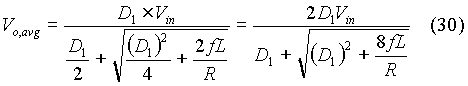
The second applet shows how D2 and Vo,avg vary when R > RC.
The first applet is shown below. It has a pull-down list of items, of which the only first item is displayed. On clicking on the downward arrow, the list is displayed. If any item of the list is high-lighted, its default value is displayed in the window adjacent to the label with the caption Set Value.. If one scrolls down or up the list, the default value of the item high-lighted is displayed in the window adjacent to the label with the caption Set Value. To change the default value of an item, highlight it first and then click inside the text-field window adjacent to the label with the caption Set Value. A line cursor would appear and the value can be changed. After changing the value, click on the Set Value label and then the program recognizes the change. It can be verified that the program has made the change out by inspecting the pull-down list again.
The default values of items in pull-down list are:
Input Voltage,dc avg = 100
Input Ripple Volt., pk-pk = 0
Input Ripple Frequency = 100
Switching Frequency,kHz = 20
Inductance, microHenry = 500
Capacitor, microFarad = 500
Load Resistance, Ohms = 10
Duty Cycle= 0.5
Slow Response,0-200 = 0.
It is possible to see one of the four responses:
Periodic response over one output cycle,
Transient response over one output
cycle,
Periodic response over one input cycle,
and
Transient response over one input
cycle.
Initially, the program sets '1' on the voltage axis of the plots equal to 100 V and sets '1' on the current axis to 10 A. If periodic response over one output cycle is chosen, the program assumes that the peak-to-peak ripple in input voltage is zero. The response can be slowed by varying the parameter called Slow Response. This parameter is effective only for periodic or transient response over one output cycle.
If the load resistance is changed from 10 W to 5 W, still '1' on the current axis would correspond to 10 A. If the Reset button is clicked, the program would make changes so that '1' on the voltage axis of the plots equal to input voltage and sets '1' on the current axis to (input voltage/load resistance).
When Start/Continue button is clicked, the
program responds to the visible response type and starts with the values
of inductor current and the capacitor voltage it had from the previous
calculation. Initially they are set to zero values. If the Reset
button is clicked, the program would make them zero again.
FIRST APPLET
The second applet takes in three parameters, namely the
switching frequency, the inductor value and the duty cycle and plots the
duty cycle of the diode and the output voltage as a function of the load
resistance varying from RC to (11 ´
RC).
SECOND APPLET
CONTROL BY PULSE-WIDTH MODULATION

The pulse-width modulator controls the semiconductor
switch and is a complex part of a switched regulator. Nowadays, switched
regulator uses a pulse-width modulator integrator circuit. The principle
of control by pulse-width modulation is illustrated in Fig. 19. The simplified
functional diagram of a typical pulse-width modulator is shown in Fig.19a,
whereas the waveforms in Fig. 19b explain the operation.
The pulse-width modulator circuit consists of a saw-tooth generator, an error amplifier, and a comparator. The frequency of saw-tooth generator can usually be set by choosing proper values of an RC network. The error amplifier compares the reference voltage and the feedback signal. The feedback signal is obtained using a voltage divider network across the output of the SMPS circuit. For example, let the feedback signal be Vf and the reference voltage be Vref. Then
![]()
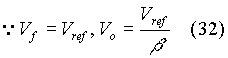
The output of the error amplifier is compared with the saw-tooth waveform and when this voltage is greater than the output of sawtooth generator, the output of the comparator would be at logic '1'. When the output of comparator is at logic '1', the switch in the SMPS circuit can be kept in the ON state. When the comparator is at logic '0', the switch in the SMPS circuit can be kept in the OFF state.
If the output voltage tends to be greater than that indicated by equation (32), the output voltage of the error amplifier would fall and the duration for which the output of comparator remains at logic '1' would decrease. Thus the duty cycle of the switch reduces and the output of the SMPS would fall, according to equation (10). Thus it can be seen that the negative feedback control maintains the output at the desired value. For negative feedback control, the feedback signal should be applied to the inverting input of the error amplifier.
When control by frequency modulation is desired, the ON-period is kept constant, but the frequency is varied in order to bring about regulation. Such a technique is necessary if the load on the regulator tends to be come very low. It is difficult to make the ON-period below a certain time duration and when this limit is reached, control by pulse width modulation becomes impossible. Then the duty cycle is reduced by keeping the ON period fixed and increasing the cycle period. The value of minimum ON period depends on the transistor switch.
In order to regulate the output voltage, a controller is needed to be designed. For this purpose, the power circuit is first represented by a transfer function.
The passive part of the power circuit is shown in Fig. 20. Since the DC output of the SMPS is defined by equation (10), the effective input to the passive circuit in Fig. 20 can be stated to be E.D(s), whereas D(s) is the Laplace transform of the output of the error amplifier shown in Fig. 19. In the design procedure outlined below, D(s) is taken to be the output of the controller, varying between 0 and 1.

For the circuit in Fig. 20,
where

The block diagram of the SMPS with a PI controller is shown in Fig. 21. The transfer functions of the different blocks in Fig. 21 are as follows:
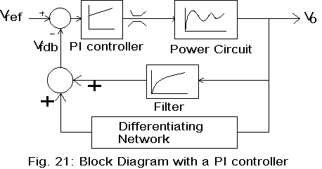
The PI controller has two inputs, the reference signal Vref corresponding to the desired output voltage and the feedback signal Vfdb. The error signal, the difference, e, between Vref and Vfdb is fed to the PI controller and the output of the PI controller is D(s), the signal that sets the duty cycle. Then
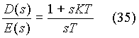
In equation (35), K is the proportional gain and T is the integrating time constant. The output of the PI controller varies between 0 and 1 and has two limits, one corresponding to the lowest duty cycle and the other corresponding to the highest duty cycle.
There is a filter in the feedback path. The filter time constant is about 4 times the cycle period corresponding to the switching frequency of the SMPS. Then the ripple at the switching frequency gets filtered out and the feedback signal is essentially a dc signal. Otherwise, the ripple in the output at the switching frequency has nearly 180o phase shift with respect to the fundamental of the input square pulse to the SMPS and then feedback at switching frequency becomes positive, which in turn leads to amplification of the ripple content. The filter avoids this problem, without seriously affecting its dynamic performance.
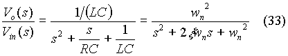
The transfer function of the power circuit is obtained as follows. Since the output varies linearly with the duty cycle, equation (33) can be presented as follows:
For designing the closed loop system, the poles due to the source can be ignored. Since the power circuit is very much under-damped, derivative feedback is required for stable operation. The differentiating circuit provides the feedback signal. For simulation, the derivative signal is obtained based on the capacitor current. The derivative feedback voltage is set to be Kd.iC.
The third applet presented below allows the user to design
a suitable PI controller. The parameters to be set are: switching frequency
in kHz, gain of the PI controller, its integrating time-constant , the
inductance, the capacitance, the load resistance, the time constant of
the filter in the feedback path and the derivative coefficient.
THIRD APPLET
The feedback arrangement used for actual simulation contains
additional circuitry. It is necessary to limit the inductor current since
it is seen from the open loop response that the inductor current can be
several times the rated current, where the rated load current is the nominal
current rating of the SMPS. It is a parameter that can be set in the program..
In this program, the current limit is set at 1.5 times the rated load current,
and when the inductor current exceeds the current limit, the current in
excess of the current limit is amplified and added to the feedback signal.
In addition, a derivative feedback signal, obtained using the capacitor
current, is added to the feedback signal. Derivative feedback improves
damping of the system and without it, the system is oscillatory in spite
of a well-designed PI controller. While designing the PI controller using
the third applet, the switching circuit is replaced by a linear amplifier
and this approximation is necessary for the design of the PI controller.
But in reality, the square-wave voltage input to the power circuit makes
the system to be oscillatory since the power circuit is heavily under-damped.
The feedback arrangement used is shown in Fig. 22.
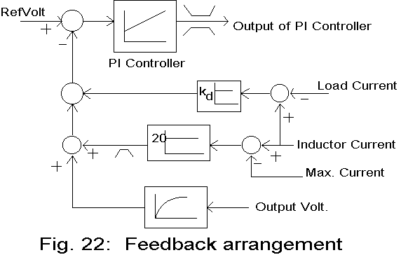
When the derivative feedback coefficient is set at unity, the derivative feedback amounts to 10% of the rated voltage when the capacitor current equals the rated current.
The fourth applet that is presented below simulates the circuit. It has a pull-down list of items, of which the only first item is displayed. On clicking on the downward arrow, the list is displayed. If any item of the list is high-lighted, its default value is displayed in the window adjacent to the label with the caption Set Value.. If one scrolls down or up the list, the default value of the item highlighted is displayed in the window adjacent to the label with the caption Set Value. To change the default value of an item, highlight it first and then click inside the text-field window adjacent to the label with the caption Set Value. A line cursor would appear and the value can be changed. After changing the value, click on the Set Value label and then the program recognizes the change. It can be verified that the program has made the change out by inspecting the pull-down list again.
The default values of items in pull-down list are:
Input Voltage,dc avg = 100
Input Ripple Volt., pk-pk = 0
Input Ripple Frequency = 100
Switching Frequency,kHz = 20
Inductance, microHenry = 500
Capacitor, microFarad = 500
Load Resistance, Ohms = 10
Output Voltage set at = 50
Gain of the PI controller = 5.
Time-constant of the PI controller
in ms =500
Time-constant of the Filter in ms
=40
Derivative Feedback Coefficient =
1.0
Rated Current in Amps = 10
Slow Response,0-200 = 0.
It is possible to see one of the five responses:
Periodic response over one output cycle,
Transient response over one output
cycle,
Periodic response over one input cycle,
Transient response over one input
cycle and
Statistics
Initially, the program sets '1' on the voltage axis of the plots equal to 100 V and sets '1' on the current axis to 10 A. If periodic response over one output cycle is chosen, the program assumes that the peak-to-peak ripple in input voltage is zero. The response can be slowed by varying the parameter called Slow Response. This parameter is effective only for periodic or transient response over one output cycle.
If the load resistance is changed from 10 W to 5 W, still '1' on the current axis would correspond to rated current. If the Reset button is clicked, the program would make changes so that '1' on the voltage axis of the plots equal to input voltage and sets '1' on the current axis to (input voltage/load resistance).
When Start/Continue button is clicked, the
program responds to the visible response type and starts with the values
of inductor current and the capacitor voltage it had from the previous
calculation. Initially they are set to zero values. If the Reset
button is clicked, the program would make them zero again.
FOURTH APPLET
MICRO-CONTROLLER IMPLEMENTATION
Nowadays the use of a micro-controller is popular. But control of a circuit switching at 20 kHz tends to be difficult, essentially due to delays involved in A/D conversion and some mathematical operations. Hence the approach to closed-loop control is a combination of rule-based logic and action of a PID controller. The delay that occurs from the instant the A/D converter samples an input signal to the instant when the corresponding digital output is available for use tends to be of the same order as the switching cycle period.
At 20 kHz, the switching cycle period is 50 mS and the delay involved due to the use of an A/D converter is about 40 mS. This means that no more than one sample can be obtained during one switching cycle period. If this sampling is done in an asynchronous manner, closed-loop can be difficult. For example, the inductor current can vary considerably over a cycle period and asynchronous sampling of inductor current may not lead to stable closed-loop control. It is preferable to sample the inductor current at a predetermined instant of the cycle period. For example, at the start of a switching cycle, a sample and hold circuit can be used to store the instantaneous value of inductor current and the A/D converter can convert this value. In the fifth applet displayed below, the A/D converter delay is set to be equal to one switching cycle period. When that is so, the sampling occurs at the beginning of each cycle. The inductor current and the capacitor voltage are sampled once in two cycles, since conversion period for each sample equals one switching cycle period.
If the sampling is to be done at a faster rate, the sampling has to be asynchronous and then an analogue filter has to be used to reduce the variations in the feedback signal corresponding to inductor current before it is used as the input to the A/D converter.
The scheme suggested for controlling the SMPS with a micro-controller is outlined with the help of a pseudo-code presented below.
Initialize:
Output Voltage Count = 0 // Output of A/D converter
Inductor Current Count =0 // Output of A/D converter
Old Current Count = 0
// Previous current count required for derivative
feedback
swCycleCount = 100
// Set the period of switching frequency as a number
of micro-controller clock frequency.
atod_delay =100
// Set the A/D converter's conversion period and
computing delay as a number of // micro-controller clock frequency.
lowCount= 5;
highCount=95;
dutyCycle=lowCount;
// Set the limits for duty cycle and set the duty
cycle at its lowest value
on_off=true;
// boolean value indicating switch is ON when it
is true
rampCount=0;
// Used with dutyCycle and swCycleCount for setting
on_off to either true or false value
atod_Count=0;
feedback Voltage=0
integrator Output=0
//Output of an integrator used in feedback control
Go to Main Loop
Main Loop:
Call Parameters Subroutine
Increment ramp Count
If (rampCount<dutyCycle) on_off = true;
Else on_off = false;
If (rampCount == swCycleCount)
{
on_off = true
rampCount=0;
}
Increment atod_Count
Increment rampCount
If (atod_Count>atod_delay) call NextValues subroutine
Return to Main Loop
Parameters Subroutine:
Begin
Desired Output Voltage=50.0
// numerical setting using
thumb-wheel switches/KeyPad
Current Limit = 125%
// Set in software, using
KeyPad or thumb-wheel switches
kd=20
// Derivative feedback coefficient
in Ohms.
// Feedback in Volt equals
(kd ´ Inductor Current).
dkI=0.1
// Integrating Coefficient
effective when output voltage is within
// a close band of ±
5% of source voltage from the desired output voltage.
End subroutine
NextValues Subroutine
Begin
atod_Count=0;
Inductor Current Count =
output of A/D output
Ouput Voltage Count = output
of A/D output
if (Inductor Current Count
<=Current Limit)
{
feedback Voltage= Ouput VoltageCoun +kd*( Inductor Current Count - Old
Current Count);
if (Desired Output Voltage>(feedback Voltage+5%)) dutyCycle++;
if (Desired Output Voltage<(feedback Voltage-5%)) dutyCycle--;
if (Desired Output Voltage>(feedback Voltage-5%)) AND (Desired Output Voltage<(feedback
Voltage+5
{
integrator output+=
dkI*(Desired output Voltage-Ouput Voltage Count)
dutyCycle+= integrator output;
if (dutyCycle<=lowCount) dutyCycle=lowCount
if (dutyCycle>=lowCount) dutyCycle=highCount
}
else
{
integrator output =0;
}
else
{
dutyCycle = dutyCycle-2;
if (dutyCycle<=lowCount) dutyCycle=lowCount;
}
End Subroutine
The fifth applet presented below simulates the operation of the switch mode step-down power supply controlled by a micro-controller. The applet has default values for the parameters listed below.
Input Voltage,dc avg = 100
Input Ripple Volt., pk-pk = 0;
Input Ripple Frequency = 100
Inductance, microHenry = 500;
Capacitor, microFarad = 500 ;
Load Resistance, Ohms = 10;
Desired Output Voltage = 50;
Rated Current, Amp = 10;
Micro's Clock Freq, MHz = 2 ;
Switching Period:Clock Cycles = 100;
A/D Delay :Clock Cycles = 100;
Derivative FeedBack Coef. =20;
Integrating Coefficient = 0.1;
This applet has the same structure as the fourth applet
and is hence not described any further.
FIFTH APPLET
IMPLEMENTATION USING A MULTIPLIER
Implementation using a multiplier is an attractive option
since this scheme can deliver nearly desired output voltage in spite of
fluctuations in the source voltage. The scheme to be used is shown
in Fig. 23.
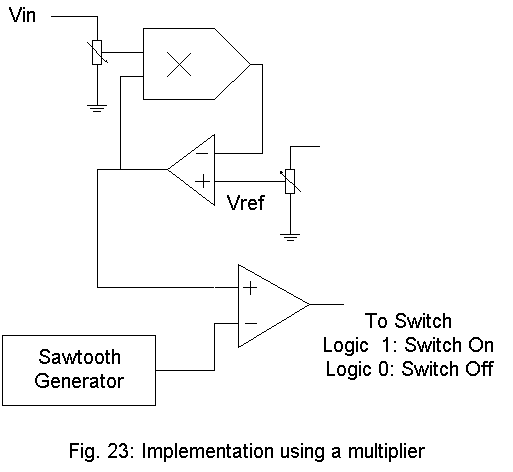
The inputs to the multiplier are the source voltage or
a part thereof and the output of the opamp in the feedback loop.
Since the output of the multiplier should equal Vref representing the desired
output voltage, the output of the opamp reflects the duty cycle.
This signal can be compared with the output of a sawtooth generator and
a pulse to turn on the switch can be obtained. If Vref can be modified
to include the effects of drop in the switch, the output of the SMPS can
equal the set value. The sixth applet simulates the SMPS controlled
in this manner.
This page has described the operation of a switch mode
step-down power supply circuit. For description in this page, it has been
assumed that the components used in the power circuit are ideal, whereas
they are not ideal in reality. The next page goes into details of the practical
limitations of the power circuit components.
![]()
![]()
![]()
![]()