The previous page on the step-down switch-mode power supply circuit was described and analyzed assuming that the components used are ideal. The real diode and the MOSFET have some limitations and they have to be taken into account for designing a practical power supply. First, the characteristics of the diode are outlined first.
DIODE REVERSE RECOVERY CURRENT
Even if a fast-recovery or an ultra-fast recovery diode
is used for free-wheeling operation, the reverse-recovery characteristic
of the diode imposes some constraints. The circuit that can be used to
test the reverse recovery characteristic of a diode is shown in Fig. 1.
An applet, named the first applet, simulates the reverse recovery property
of the diode and is displayed below.

The operation of the test circuit is explained at first. The time constant due to load inductance and load resistance should be several times the time corresponding to the switching frequency. Then the current through the remains more or less steady and its value is given by:

When the MOSFET is ON, the load current flows through the transistor. When it is turned off, the current flows through the snubber circuit initially and then the free-wheeling diode, marked as DUT (device under test). When the MOSFET is switched ON again, the source tends to reverse the current through the diode. The current through the diode falls rapidly and reverses before it becomes zero. The reverse recovery has been simulated using the model of the diode shown in Fig. 1.
The reverse-recovery transient process depends on the diode itself and it also depends on the junction temperature of the diode, the forward current prior to being reverse biased, the rate of fall forward current and the source voltage that applies to the reverse bias to the diode. As the value of any one of these parameters rises with the other parameters remaining unchanged, the reverse recovery transient process becomes worse, reflected by an increase in the peak reverse current. The reverse recovery turn-off period starts once the diode current becomes negative and lasts till the reverse diode current increases in ampltidue first and then decays to about 10% of its reverse peak current. It represents the time that has to elapse before the diode recovers ability to block reverse voltage.
The manufacture specifies the reverse recovery transient period and the maximum reverse current for a set defined by its forward current, the rate of fall of forward current and the junction temperature. For many diodes, the maximum rate of fall forward current is specified to be 100 A/ms. This means the test inductance L should set be such that
If reverse recovery transient is to be minimized, it would be preferable to select L such that
where the rated current of diode is Irated,diode and trr is its reverse recovery transient period.
The applet simulates the reverse recovery transient. It is an approximation of the behaviour of the diode. No accuracy for this model is claimed, but it does show the dependence of recovery transient on the parameters mentioned. The pull-down choice menu contains rated current of the diode, its turn-off period, its turn-on period, load current, source voltage, test inductance in nH, test resistance in Ohms and the junction temperature as its items. To change the value of a menu-item, pull down the menu, highlight the item, change its value in the adjacent text-field and then click on Set Value button. When the Run/More button is clicked, the program displays the diode current and the voltage across the diode for a period corresponding to 12 times the turn-off period. If the diode had not turned off by then, click again on the Run/More button, and the process that occurs for the next 12 times the turn-off period would be displayed. Whenever the rate of fall of forward current increases due to either lower test inductance or higher source voltage, the total period required for the diode to turn-off decreases, but there would a significant increase in the peak reverse current.
APPLET FOR REVERSE RECOVERY TRANSIENT
IN A DIODE
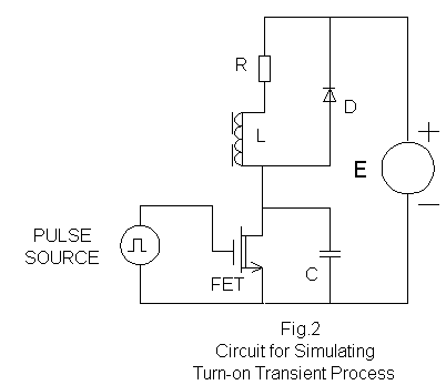
The turn-on transient in a diode is not as predominant as its turn-off process is, but nonetheless it affects the performance of the circuit in which it is placed. The circuit for simulating the turn-on transient process is shown in Fig.2 and the diode model used is the same as shown in Fig. 1.
In a practical circuit, it is often difficult to notice
the turn-on transient process, for two reasons. Firstly, the turn-on process
lasts only for a brief period. Secondly, the transient process of some
other device can often mask the turn-on process of a diode. For example,
the turn-off delay of the MOSFET can mask the turn-on process of the diode.
The simulation, shown in the second applet, makes the assumption that the
transistor is ideal and simulates the turn-on process in an approximate
manner.
In some circuits, such as the flyback converter to be described in one of the pages to follow, the turn-on delay of the diode is crucial. The only practical remedy to address this problem is to connect an RC snubber circuit across the diode.
APPLET FOR TURN-ON TRANSIENT
IN A DIODE
TRANSIENT PROCESSES IN A MOSFET
For a MOSFET, three transient processes can be identified. The first is the turn-on transient process associated with the MOSFET and the second is its turn-off process and the third is the turn-off transient process associated with the body-diode of the MOSFET. The turn-on transient of the body diode is relatively fast and can be ignored.
For a fast MOSFET, the turn-on transient process is characterized by two time periods, one is the turn-on time delay and the second is the rise time. During the turn-on time delay, the gate-to-source voltage builds up to its threshold value and during the rise time, the device current rises to about 90% of its final value. There is a further delay before the drain-to-source voltage becomes equal to its conduction drop. The delay time can be reduced to some extent by a stiff gate drive signal. When the MOSFET is turned off, there is a delay period corresponding to the period in which the gate voltage reduces to its threshold level. Then the cross-over period that includes a delay period and a fall period. During the delay period, the drain-to-source voltage rises from its conduction value to its blocking value. After this delay period has elapsed, the fall period follows during which the current through the MOSFET decreases. For a fast MOSFET, the total turn-on transient lasts for about 50 ns, whereas the turn-off process lasts for about 100 ns.
The body diode is comparatively slow. It turns on quite fast, but its turn-off process is quite slow, of the order of 500 ns. Hence when the MOSFET is to be operated at high frequency, it is preferable to use an external diode. In such a case, an additional diode may be required, that has to be connected in series with the MOSFET.
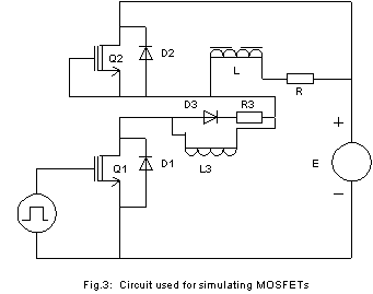
A circuit that can be used for simulating the transient
processes in a MOSFET is shown in Fig. 3. Here Q1 is turned on and off,
whereas Q2 remains off. When Q1 is turned off, the load current is diverted
through diode D2, the body diode of Q2 . When Q1 is turned on, both the
turn-on transient of Q1 and the reverse recovery transient of D2 occur.
The simulation that is displayed as applet 3 is again quite approximate.
The purpose is to illustrate how MOSFET functions as a switch. An air-cored
inductor, labeled L3 in Fig.3, is necessary to be used to reduce the reverse
recovery current of the diode. The time constant due L3 and R3 should be
much less compared with the cycle period corresponding to switching frequency.
The turn-on process of the MOSFET is quite slow, due to the slow turn-off
of the body diode D2. In applications where the MOSFET has to be switched
on and off at higher frequency of the order of 20 kHz and above, it is
the practice to bypass the body diode by an external diode. In this application,
such a technique is unnecessary because the body diode does not have to
conduct at all.
APPLET FOR TRANSIENT PROCESSES IN A MOSFET
The losses in a FET are due to three factors:
LOSSES IN ENERGY STORAGE ELEMENTS
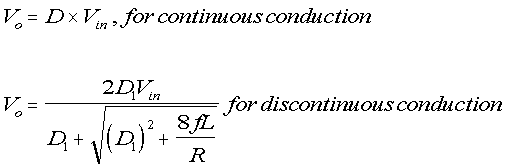
The non-ideal properties of filter capacitor at the output and the inductor affect the performance of the circuit. The inductor is not lossless because of the winding resistance and the core loss. The model of the inductor can be changed to a series network containing a resistor reflecting its losses and an inductor. Due to the losses in the inductor, there is a slight reduction in the output voltage and also a drop in the efficiency of the circuit. Given a duty cycle and a steady input voltage, the output voltage is has been obtained in the previous page as:
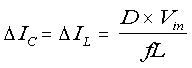
The average inductor current is the same as the average load current. Then the average inductor current IL is:

If the internal resistance of the inductor is Rind, the drop in output voltage is approximately:
![]()
The effect of the ESR of capacitor is to increase the
ripple content in output. From the previous page, the change in capactor
current from its higheest value to its lowest value is:
The worst-case increase in peak-to-peak ripple in output
voltage can be obtained by just adding the ripple due to ESR with the previously
obtained value. If ESR of capavitor be Rcap, then
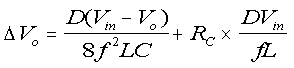
The actual peak-to-peak ripple would be less than the value stated above.
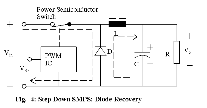
It is necessary to modify the step-down SMPS if it is to operate at relatively high voltage in the continuous conduction mode. The problem with continuous conduction occurs when the MOSFET is turned on with the diode still in conduction. To explain this aspect, Fig. 4 is presented. When the MOSFET is turned on, the diode can act as a short circuit till it recovers. To overcome this problem, the circuit in Fig. 4 is to be modified.
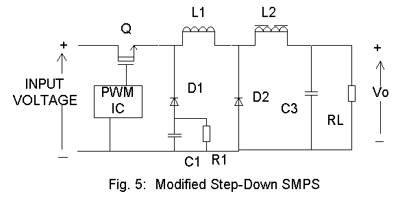
The modifed circuit is presented in Fig. 5. This circuit, when designed properly, would well whether the conduction is continuous or discontinuous. This circuit contains a few additional components. The components added are an additional diode marked as D1, an RC snubber circuit for D1, a capacitor labeled as C2. Diode D3, inductor L2 and capacitor C3 are the same components, marked as D, L and C respectively in Fig. 4. The operation of the circuit in Fig. 5 is explained now.
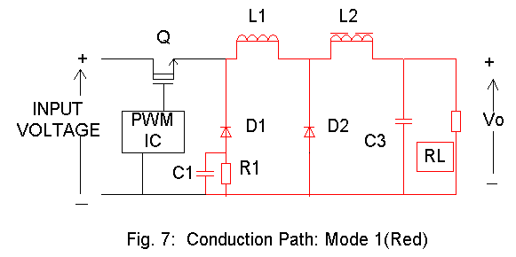
The conduction path that exists when the MOSFET is ON
is shown in red colour in Fig. 6. The current flow is through the MOSFET
and the inductors.

When the MOSFET is turned off, the set of components in
conduction varies. In mode 1 following immediately after the turn-off of
the MOSFET, diode D1, inductor L1, capacitor C1, resistor R1 and components
L2 C3 and RL are in conduction. The RC circuit in series with D1 conducts,
the time constant associated with C1 and R1 being very small compared with
the on-off periods of the MOSFET. During this mode, inductor L1 discharges
its energy to R1 and C1. The components in conduction in mode 1 are shown
in Fig. 7.
When mode 1 is over after inductor L1 has discharged its
energy, mode 2 follows. Here only D2 continues to conduct, but L1 and D1
are not in conduction. This mode is illustrated in Fig. 8. During this
phase, C2 would discharge any energy it may have acquired into R2. After
the end of the period corresponding to the switching frequency, the MOSFET
is turned ON again and the circuit reverts to the state shown in Fig. 9.

The circuit lasts in the state shown in Fig. 9 till the
current through L1 becomes equal to that through L2. After that, the circuit
reverts to the state shown in Fig. 6.

When the MOSFET is switched on, current through L1 rises gradually and current through D2 falls gradually. If inductor L1 is sufficiently large, there would be hardly any reverse recovery transient due to diode D2. Typically L1 should be such that the rate of rise current is less than 25% of the maximum rate of fall specified for diode D2. Inductor L1 can even be an air-core inductor, whereas inductor L2 has a ferrite-core with an air gap.
The fourth applet presented below simulates the circuit in Fig. 5. It is assumed that the turn-on delay of diodes is negligible. The puul-down menu contains two items that are not shown explicitly in Fig.5. They are the equivalent-series resistance of capacitor C3 and the internal resistance of inductor L2. In practice, even with a fixed duty cycle, a fixed switching frequency and a steady-input voltage, the ripple content in output tends to be higher than the calculated value, mainly due to the ESR of C3. The default value of ESR of C3 is set to be zero. To see its effect, the type of response should be set as Statistics. Then when the program is run, the peak-to-peak ripple in output voltage is displayed. The program has to be run a few times in this mode before the peak-to-peak ripple in output settles down to its periodic value. For example, when ESR of C3 is increased to 0.1 W , it can be seen that the peak-to-peak ripple that results is much higher.
The internal resistance of L2 reflects the winding resistance and the core loss and the losses in inductor L2 tend to reduce the efficiency of this converter. The default value of internal resistance has been set to be zero. Its realistic value can be calculated by assuming a quality factor of about 100 at the switching frequency. For the value of inductor L2, an appropriate value of internal resistance of L2 can be set to be about 0.5 W. To see its effect, the type of response should be set as Statistics in the program.
When the type of response is Statistics,
the program should be run a few times before the results become repetitive.
Even then, the sum of output power and all the losses may not add upto
the input power, due to
errors in modelling and the presence of energy storage
elements. The loss calculation of diode D1 in particular is
quite incorrect, because the turn-on losses of a diode have been ignored.
Even though the average current of D1 turns out to be small, its turn-on
losses are quite significant and it is advisable to use the same diode
selected to be used as D2. These diodes should be fast-switching
diodes with a low reverse period of about 50 ns.
APPLET FOR PRACTICAL BUCK
CONVERTER IN FIG. 5
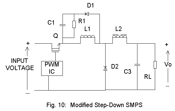
The modified circuit shown in Fig. 5 is better than the ideal circuit, since it tries to fix the problem that arises due to the reverse recovery transient in diode D2. The modified circuit in Fig. 5 works well so long as inductor L1 is large enough to prevent diode D2 from going into reverse recovery transient process. It can be seen from the applet for reverse recovery transient in a diode that there is hardly any reverse recovery current if the test inductance is large. If L1 shown in Fig. 5 is not large enough, the modified circuit's behaviour is unpredictable. When the MOSFET turns ON, current through L1 builds up and current through D2 falls, with hardly any change in current through L2. When the current through D2 becomes zero too soon, there would stille be charge carriers trapped inside D2 and it would continue to conduct. The rise in reverse recovery current would be restricted by L1, but when D2 snaps into off condiction, the current in L1 could be larger than that in L2 and then we have a circuit with a potential danger. If there be nod path for excess current in L1, there would be a voltage transint due to L1, which in turn can lead to damage of either the MOSFET or diode D2 or both. This problem can be averted by repositioning D1, R1 and C1 as shown in Fig. 10. This circuit behaves exactly in the same way as the circuit in Fig. 5, except that it has a built-in mechanism to handle the problem described above. In case when the current through L1 is higher than L2 when diode D2 snaps off, the excess current can free-wheel though D1, R1 and C1. The circuit in Fig. 10 is the recommended modified circuit.
CURRENT MODE CONTROL: IDEAL CIRCUIT
Current mode control of a SMPS is a popular technique built into several PWM integrated-circuits nowadays. This topic should have been covered in the previous page, but has been held over and presented now.
The block diagram of the current-mode control is similar to that described the previous page on the ideal step-down SMPS circuit. The PI controller illustrated in Fig. 22 of the previous page can used be as it is. In the previous page, closed-loop control was effected by comparing the output of the PI controller with a ramp signal (Fig. 19). For current-mode control, the output of the PI controller should be compared with the signal reflecting the current though the inductor L2, with this signal suitably scaled. This signal is compared with the PI controller output and when the signal corresponding to inductor current tends to exceed the PI controller output, the MOSFET is turned off for the rest of the output cycle. At the start of each cycle, the MOSFET should be turned on.
With just this type of control, the pulse-width tends
to fluctuate from one cycle to the next, leading to oscillations in output.
Ideally duty cycle should be equal to the ratio of desired output
voltage to the source voltage, but the intersection of the PI controller
output and the signal reflecting inductor current may not always occur
after a time lapse from the start of a cycle that corresponds to the desired
duty cycle. To overcome this problem, a component proportional to
the time elapsed from the instant the cycle starts can be added to the
signal corresponding to the inductor current and this sum can be compared
with the output of the PI controller. Let us say that the maximum
of the PI controller output be 10 V and let the signal corresponding to
inductor current be 10 V when the inductor current is at nominal rated
value. Let also a ramp voltage be generated such that it rises from 0 V
to 10 V from the start to the end of a cycle. Then a fraction of
the ramp voltage can be added to the signal reflecting current, the fraction
being equal to the duty cycle which in turn is the ratio of desired output
voltage to the source voltage. When the source voltage tends to vary
over an input cycle, this fraction computed as the ratio of desired
output voltage to the source voltage automatically gets adjusted and the
correction to the signal reflecting the inductor current becomes the right
adjustment.
APPLET FOR PWM WITH CURRENT
CONTROL
This page has described the practical aspects of the step-down SMPS. The inductor design for the SMPS is also critical and it is described in one of the pages to follow.
The next page describes the operation of the step-up switch-mode
power supply circuit.