
INTRODUCTION
ANALYSIS OF THE IDEAL CIRCUIT
CONTINUOUS CONDUCTION
DISCONTINUOUS CONDUCTION
CLOSED-LOOP CONTROL USING PWM
IMPLEMENTATION USING A MULTIPLIER
CURRENT-MODE CONTROL
MICRO-CONTROLLER IMPLEMENTATION
SUMMARY
The boost converter, also known as the step-up converter, is another switching converter that has the same components as the buck converter, but this converter produces an output voltage greater than the source. The ideal boost converter has the five basic components, namely a power semiconductor switch, a diode, an inductor, a capacitor and a PWM controller. The placement of the inductor, the switch and the diode in the boost converter is different from that of the buck converter. The basic circuit of the boost converter is shown in Fig. 1.
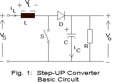
The operation of the circuit is explained now. The essential control mechanism of the circuit in Fig. 1 is turning the power semiconductor switch on and off. When the switch is ON, the current through the inductor increases and the energy stored in the inductor builds up. When the switch is off, current through the inductor continues to flow via the diode D, the RC network and back to the source. The inductor is discharging its energy and the polarity of inductor voltage is such that its terminal connected to the diode is positive with respect to its other terminal connected to the source. It can be seen then the capacitor voltage has to be higher than the source voltage and hence this converter is known as the boost converter. It can be seen that the inductor acts like a pump, receiving energy when the switch is closed and transferring it to the RC network when the switch is open.
When the switch is closed, the diode does not conduct and the capacitor sustains the output voltage. The circuit can be split into two parts, as shown in Fig. 2. As long as the RC time constant is very much larger than the on-period of the switch, the output voltage would remain more or less constant.

When the switch is open, the equivalent circuit that
is applicable is shown in Fig. 3. There is a single connected circuit in
this case.

Analysis of the circuit is carried out based on the following assumptions. The circuit is ideal. It means when the switch is ON, the drop across it is zero and the current through it is zero when it is open. The diode has zero voltages drop in the conducting state and zero current in the reverse-bias mode. The time delays in switching on and off the switch and the diode are assumed to be negligible. The inductor and the capacitor are assumed to be lossless.
When the switch is closed, the equivalent circuit that is applicable is shown in Fig. 2. The source voltage is applied across the inductor and the rate of rise of inductor current is dependent on the source voltage VS and inductance L. The differential equation describing this condition is:
If the source voltage remains constant, the rate of rise of inductor current is positive and remains fixed, so long as the inductor is not saturated. Then equation (1) can be expressed as :

The switch remains ON for a time interval of DT in one switching cycle and hence DT can be used for )t. The net increase in inductor current when the switch is ON can be obtained from equation (2) to be:
Inductor Current with Switch Open
When the switch is open, the circuit that is applicable is shown in Fig. 3. Now the voltage across the inductor is:
![]()
Given that the output voltage is larger than the source voltage, the voltage across the inductor is negative and the rate of rise of inductor current, described by equation (5), is negative. Hence if the switch is held OFF for a time interval equal to (1 - D)T, the change in inductor current can be computed as shown in equation (6)
 .
.
The change in inductor current reflected by equation (6) is a negative value, since Vo > VS. Since the net change in inductor current over a cycle period is zero when the response iL(t), the sum of net changes in inductor current expressed by (4) and (6) should be zero. That is,
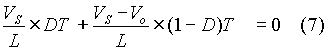
On simplifying equation (7), we get that

It has been stated that when iL(t) is periodic, the net change in inductor current over a cycle is zero. Since change in inductor current is related to its volt-seconds, the net volt-seconds of the inductor has to be zero. The expression for the net volt-seconds can be obtained from equation (6) and it can be seen that the numerator of equation (7) should be zero. That is,
![]()
The value of D varies such that 0 < D < 1 and it can be seen from equation (8) that output voltage is greater than the source voltage, and hence this circuit is called the boost converter. The output voltage has its lowest value when D = 0 and then the output voltage equals the source voltage. When D approaches unity, output voltage tends to infinity. Usually D is varied in the range 0.1 # D # 0.9 .
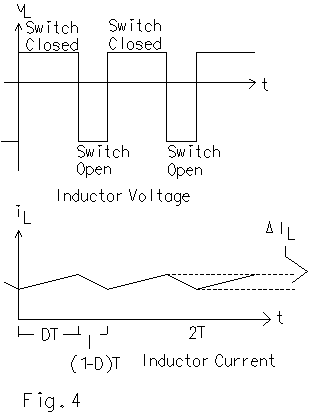
The waveforms of inductor voltage and inductor current are shown in Fig. 4. These waveforms are drawn assuming that both the output and the source voltage remain steady. These waveforms illustrate how the inductor voltage is related to its current.
Output Voltage Ripple with Switch Closed
In this sub-section, the change in output voltage is calculated. It needs to be emphasized that the peak-to-peak ripple in output voltage is quite small for a well-designed circuit. For the inductor, the net change in inductor current over a cycle is zero when iL(t) is periodic. For the capacitor, the net change in capacitor voltage over a cycle is zero when it is periodic. When the switch is closed, the equivalent circuit in Fig. 2 shows that the boost converter is split into two sub-circuits, with the loop currents decoupled from each other. When the switch is closed, the output voltage is sustained by the capacitor. During this period, the capacitor discharges part of its stored energy and it re-acquires this energy when the switch is open. When the switch is open, part of the inductor current charges the capacitor since the inductor current usually remains larger than the current through the load resistor. From Fig. 2,
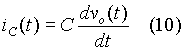
When current through a capacitor charges it up, its rate of rise of capacitor voltage is positive since the capacitor voltage is increasing. When the switch is open, the capacitor is discharging its energy with its voltage falling and the current through the capacitor is then a negative value. The output voltage remains positive and hence the output current is positive and it is the negative of the capacitor current, as can be seen from Fig. 2. Since the change in output voltage is quite small, it can be assumed that the load current remains constant at its average value and equation (10) can be now expressed as:

When the capacitor current is constant, its voltage changes linearly with time. Here the period for which the switch is closed is DT and the DT can be used in place of )t and the peak-to-peak ripple in output voltage expressed as )vo is then:
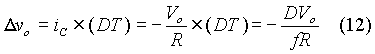
Equation (12) yields the value of the peak-to-peak ripple in output voltage. In equation (12), 1/f replaces T since T is the reciprocal of switching frequency.

Figure 5 shows how the capacitor current and voltage vary over a cycle. The ripple in output voltage is exaggerated in Fig. 5, whereas in practice it would be much smaller. If the output voltage is drawn to scale, the ripple in output voltage would not be noticeable.
Expression for Average Inductor Current
The average inductor current can be found out by equating the power drawn from the source to the power delivered to the load resistor. Again the ripple in output voltage is ignored and it is assumed justifiably that the output voltage remains steady at its average value. Power Po absorbed by load resistor is then:
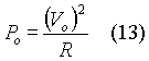
It can be seen from the circuit in Fig. 1 that the current drawn from the source flows through the inductor. Hence the average value of inductor current is also the average value of source current. Let the average inductor current be IL. Then power PS supplied by the source is then:
![]()
After equating equations (13) and (14), we get the average inductor current as:
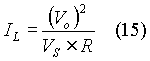
Since load current Io is:

Using equations (8) and (16), equation (15) can be re-presented as:
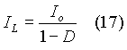
Since 0 < D < 1, it can be seen from equation (17) that IL > Io.
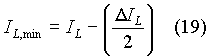
The analysis thus far is based on the assumption that the current through the inductor is continuous. The inductor current varies over a cycle, varying between a minimum value and a maximum value. The minimum and maximum values can be expressed in terms of its mean value and its change as expressed in equation (3). That is,

and
It is shown in Fig. 6 how the maximum and the minimum
inductor current can be obtained. It is also shown that as the load resistor
becomes greater, the average inductor current reduces, but the peak-to-peak
ripple in inductor current does not change. It has to be so and expression
for DIL in equation (3) does not
indicate any term reflecting the load resistor.

For continuous conduction,

At the boundary of continuous and discontinuous conduction,

Another expression for IL is now obtained. Substituting for Vo in equation (15) the expression in equation (8), we obtain that
Substituting for IL from the equation above and for )iL from equation (3), equation (18) becomes:
and
From equations (23) and (24), the condition for continuous conduction is:

Equation (25) can be interpreted as follows, assuming that only one of the four parameters is varied at a given time with the other three parameters remaining unchanged.
The circuit tends to become discontinuous,
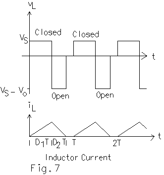
When the conduction is discontinuous, the voltage across the inductor is zero for part of the cycle since there is no current through the inductor. Let D1T be the time for which the switch is ON in one cycle and let D2T be the period for which the diode conducts. Since the conduction is discontinuous,
![]()
An expression for the output voltage can be obtained in terms of source voltage, duty cycle D1 of the switch and duty cycle D2 of the diode. Since the net change in inductor current is over a cycle, the net volt-seconds area associated with the inductor is zero. The waveforms relevant to the inductor when the conduction is discontinuous are shown in Fig. 7. From Fig. 7,
![]()
On simplifying, an expression for Vo can be obtained. Then

The value of D1, the duty cycle of the switch, is usually known, but the period for which the diode conducts is an unknown quantity depending on the other circuit parameters. The value of D2 can be determined in several ways. Here it is determined using the power balance between the input and output. When the circuit is ideal, the input power equals output power. Let the average source current be IS and the average output current be Io. Then
![]()
Using equation (28), we get that
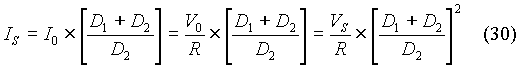
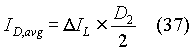
The average source current be IS can be obtained from Fig. 7. The average source current is the same as the average inductor current. Let the peak inductor current be DIL and the period for which this current flows is (D1T + D2T). This period is the base of the triangle that defines the inductor current. The average inductor current is obtained as the area of this triangle divided by the cycle period. We have that
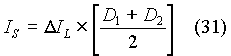
Equating equations(30) and (31),
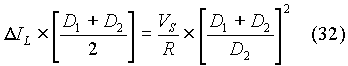
From equation (3),
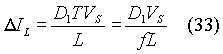
Substituting for DIL from equation (33) in equation (32), we get that
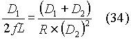
Equation (34) can be re-written as:

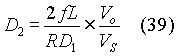
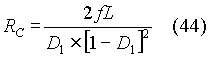
Solving for D2,

Equation (36) states how D2 varies as a function of R, D1 , f and L. Once D2 is known, Vo can be obtained from equation (28).
It is possible to get an expression for Vo as a function of R, D1 , f and L. For this, we equate the average load current with the average diode current. The average output current can be obtained from the average output voltage and the load resistor. The average diode current is:
Using the expression for DIL from equation (33), and replacing the L.H.S. by the average load current,

Hence we obtain that
By substituting for D2 from equation (36) in the above equation, we can get an expression for Vo/VS. Alternatively, equation (28) can be re-written as:

Using the expression for D2 from equation (39) in equation (40),
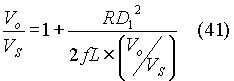
That is,
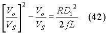
Solving for the ratio of output to source voltage and taking the positive root of the expression on the R.H.S. of equation (42),

Equation (43) states how (Vo/VS) varies as a function of R, D1 , f and L
Two applets are presented below, the first applet simulates the behaviour of the ideal circuit in open loop, whereas the second applet is about the discontinuous mode of operation.
The first applet presents four types of responses. When the circuit is switched on at a fixed duty cycle with no energy stored in either the inductor or capacitor initially, the transient inductor current happens to be large. If the input voltage has any ripple content, its effect can be seen by selecting either the periodic response or the transient response over one input cycle.
The second applet displays two sets of curves. The first set illustrates how the ratio of output voltage to input voltage varies as a function of the ratio of load resistance to critical resistance for different duty cycles of the switch, where the critical resistance is calculated from equation (25). The critical resistance at a given duty cycle can be stated to be:
The second set of curves illustrates how the duty cycle of the diode varies as a function of the ratio of load resistance to critical resistance for different duty cycles of the switch. The values of critical resistance at various values of duty cycle are also displayed. The parameters to be set initially are the frequency of operation and the value of inductor.
Under this section, the closed-loop control of the ideal circuit is considered. For both the buck converter and the boost converter, the output voltage increases as the duty cycle of the switch increases and hence the same PWM circuit can be used. The block diagram is also similar, but the transfer function is only slightly different. The block diagram is shown in Fig. 8.
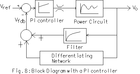
A more detailed block diagram is shown in Fig. 9.

The transfer function of the circuit in open loop is obtained as outlined below by using an approximate method. Even though it is difficult to justify the approximation, it is presented. The output voltage is expressed by equation (8). Let the quiescent duty cycle be assumed to be D and let the small increment to duty cycle be d. Then equation (8) can be presented as:
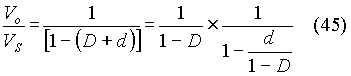
If d<< (1-D), then the above equation can be approximated using the binomial expansion and retaining only the first two terms. That is,
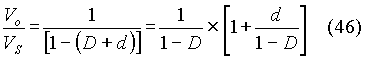

The change in output, denoted as DVo, can be expressed to be
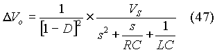
The transfer function can then be obtained as:

The design of the controller is based on the block diagram
in Fig. 10. The third applet has been developed based on this block diagram.
The difference between the inductor current and the load current is the
capacitor current and the current through the capacitor is proportional
to the derivative of the capacitor voltage and the derivative feedback
is obtained as shown. . The third applet presented below displays the location
of poles and zeros for the selected parameters. If any poles happen to
be in the right-half side of s-plane, the program may not work
For simulation of the power circuit using PWM, closed loop scheme used is shown in Fig. 9. As long as the inductor current is less than the maximum current, the feedback signal is the sum of the output voltage filter output and a derivative signal obtained from the inductor current and the load current. When the inductor voltage exceeds the set maximum value, the feedback signal contains an additional element proportional to the amount by which the inductor current exceeds the maximum current. The output of the PI controller determines the duty cycle.
The simulation of the power circuit with closed-loop control and pulse-width modulation mode is presented in the fourth applet. One of the five responses can be selected and the program interface is similar to many of the preceding applets.
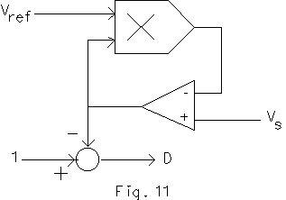
IMPLEMENTATION USING A MULTIPLIER
It is possible to use a multiplier for boost converter also. Using equation (8), an expression for the duty cycle can be obtained to be:
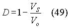
The above equation is valid if the conduction is continuous. The above equation can be realized using a multiplier and a few opamps as shown in Fig. 11. It needs to be mentioned that components should be chosen suitably, reflecting the required scaling. For example, if the multiplier yields an output of 10 V when both its inputs are at 10 V, an input of 10 V should correspond to the maximum input voltage. If the maximum duty cycle is set to be 0.9 and it corresponds to 9 V, then an input of 9 V to the opamp in the feedback path should correspond to the maximum desired output voltage. In this case, the ramp signal with which the output of this circuit is compared should rise from 0 V to 10 V in one cycle period. Based on this scaling scheme, a value of unity in Fig. 10 corresponds to 10 V. Instead of using Vo, a reference signal proportional to desired output is used in Fig.11.
Current-mode control of buck converter has been described in the previous page. The method to be used for boost converter is more or less the same. Here also slop compensation is needed in order to ensure stability. Compensation to be added to signal reflecting inductor current is a fraction of the ramp signal, where the fraction is computed according to equation (49). The sixth applet that follows simulates the boost converter circuit with current-mode control. The program may take a while to display periodic responses, whereas transient responses are displayed with no significant delay.
MICRO-CONTROLLER IMPLEMENTATION
The program used for micro-controller implementation is the more or less the same as that used for buck converter. Since the boost converter circuit is more under-damped than the buck converter circuit is, the responses obtained display behaviour associated with under-damped systems. Hence the program may fail to compute periodic responses with consequent delay, whereas transient responses are displayed with no significant delay.
This page has described the operation of the ideal boost
converter. The next page explains the problems associated with this circuit
and describes a solution to build a reliable boost converter. The next
page describes also an application of the boost converter.