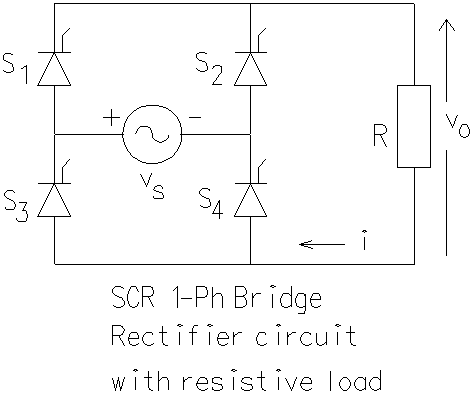
The analysis is relatively simple when the load is purely resistive. The aims of the analysis are:
i. To obtain
the average output voltage as a function of firing angle,
ii. To obtain the
rms output voltage as a function of firing angle,
iii. To obtain the ripple
factor of output voltage,
iv. To obtain the rms line
current,
v. To obtain the
fundamental component of line current,
vi. To obtain the Displacement
power factor and power factor of line current and
vii. To obtain the total harmonic
distortion(THD) in line current.
The average value of the output voltage is obtained as follows. Let the supply voltage be vs = E*Sin (q ), where q varies from 0 to 2p radians. Since the output waveform repeats itself for every half-cycle, the average output voltage is expressed as a function of a, the firing angle, as shown in equation (1). The r.m.s. value of output voltage is obtained as shown in equation (2). The ripple factor in output voltage can defined in two ways. The definition followed in this text as follows. The maximum average output voltage occurs at a firing angle of 0o. Let it be Vom. Then the ripple factor RF(a) is defined as shown in equation (3).
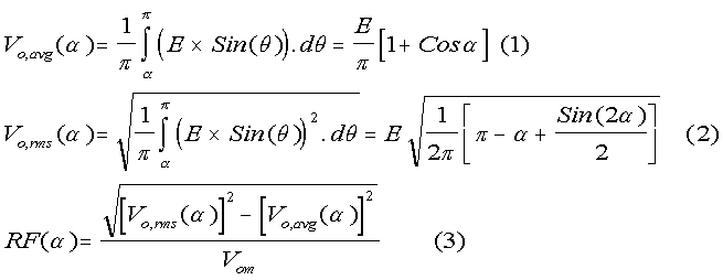
The alternate definition uses Vo,avg(a) as the denominator instead of Vom. If Vo,avg(a) is used as the denominator, then RF(a) can tend to infinity. It is more logical to express the ripple content as a fraction of the maximum average voltage. The variation of average output voltage, rms output voltage and ripple factor with the firing angle have been shown below. The plots shown below have been normalized with respect to Vom. For example, when the firing angle is 90o, the average output is shown to be 0.5. It means that the actual average output voltage is 0.5Vom. It can also be seen that when the firing angle is 0o, the r.m.s. output voltage is about 1.1Vom and the ripple factor is about 0.48. The ripple factor increases as the firing angle increases. It increases to 0.658 at a firing angle of 65o and then it falls as the firing angle increases further. At the firing angle of 65o, the r.m.s. ripple voltage in the output is 0.658Vom. For a sinusoidal source of 240 V r.m.s., the maximum r.m.s. ripple voltage works out to be 142 V.
PERFORMANCE PARAMETERS FOR CONVERTERS
The role of a rectifier circuit is to produce a dc output voltage from an ac sinusoidal source. The rectifier's output is not pure d.c. and it contains ripple superimposed on its d.c. content and the current drawn from the ac source is not sinusoidal either. It contains some fundamental component and harmonics. For the output voltage, its ripple content is the performance criterion. It would be desirable to obtain the amplitude frequency spectrum of the output of the rectifier in order to design a suitable filter circuit. However there is no mention of how to design a filter in this page.
As far as the ac source is concerned, the distortion in the source current is the performance criterion. The total harmonic distortion(THD) or the harmonic factor, the amplitude frequency spectrum of the source current, the apparent power factor and the displacement power factor have also to be computed. In addition, the crest factor is also to be computed, to facilitate the selection of the proper SCR.
Given a periodic function f(t) with a period of T, f(t) can be described by a trigonometric Fourier series, as shown in equation (4). The coefficients are defined as shown in equations (5), (6) and (7).

In the equations above, * is used to in place of the product sign and it should not be confused with the same symbol used for indicating convolution integrals. The source frequency, f, is taken as the fundamental and hence wo = 2pf. It is preferable to express the above equation in terms of angle q, where q = wot. If T is the cycle period, woT = 2p fT = 2p, since f = 1/T. Then the equations for the Fourier coefficients can be expressed as shown in equations (8), (9) and (10).

In the case of the full-wave bridge rectifier circuit, the period of the output is only half that of the input sinusoidal source and hence the output contains a dc component and even harmonics only. The source current has half-wave symmetry. A waveform defined as f(t) over a cycle is said to have half-wave symmetry if it satisfies equation (11). A waveform with half-wave symmetry contains a fundamental component and odd harmonics only.
Let the Fourier coefficients for the output voltage be av0(a), av2n(a) and bv2n(a) , where a is the firing angle and these coefficients are evaluated as shown in equations (12), (13) and (14). Since the output repeats itself twice for every cycle of source voltage, it contains only even harmonics. Then we obtain the amplitude of the harmonic as shown in equation (16).
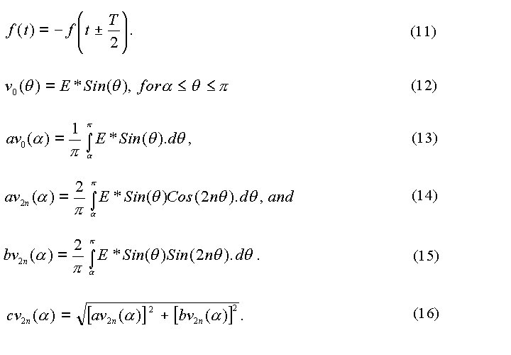
Let the Fourier coefficients for the source current be acur0(a), acur2n(a) and bcur2n(a) . The line current waveform has half-wave symmetry and contains only odd harmonics. When the SCRs are assumed to be ideal, load current iLine(q) is defined by equation (17).

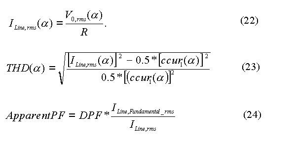
For the case where the load is purely resistive, the r.m.s. source current can be computed from the value obtained for the output voltage, as shown in equation (22). Then the total harmonic distortion is defined by equation (23). Let the r.m.s current when the firing angle is 0o be Irms,max. Since the waveform of the source current is purely sinusoidal when the firing angle is 0o, the crest factor can be taken to be square root of 2. The program that simulates the operation of this circuit computes the various values for a given firing angle and displays them in a suitable manner.
The displacement power factor, DPF, is the cosine of the angle by which the fundamental component of the line current lags the source voltage. Then apparent power factor can be estimated as shown in equation (24).
The firing angle has to be keyed-in. Then click on Compute button. The plots for voltage have been normalized with respect to Vom and the currents with respect to Irms,max. The statistical details related to the output voltage have been normalized with respect to Vom and those related to the source current with respect to Irms,max. The amplitude of each harmonic in the output voltage has been normalized with respect to E which is the amplitude of the source voltage , whereas the amplitude of each harmonics in the source current has been normalized with respect to E/R.
The circuit used for Pspice simulation is shown below. All the nodes other than the datum node are connected to the datum node through a 1 MW resistor. A floating node or a node that tends to float can be a problem for Pspice simulation.

The program is presented below.
* Full-wave Bridge Rectifier with a resistive load
VIN 1 0 SIN(0 340V 50Hz)
XT1 1 2 5 2 SCR
XT2 0 2 6 2 SCR
XT3 3 0 7 0 SCR
XT4 3 1 8 1 SCR
VP1 5 2 PULSE(0 10 1667U 1N 1N 100U 20M)
VP2 6 2 PULSE(0 10 11667U 1N 1N 100U 20M)
VP3 7 0 PULSE(0 10 1667U 1N 1N 100U 20M)
VP4 8 1 PULSE(0 10 11667U 1N 1N 100U 20M)
R1 2 3 10
R2 1 0 1MEG
R3 2 0 1MEG
R4 3 0 1MEG

* Subcircuit for SCR
.SUBCKT SCR 101 102 103 102
S1 101 105 106 102 SMOD
RG 103 104 50
VX 104 102 DC 0
VY 105 107 DC 0
DT 107 102 DMOD
RT 106 102 1
CT 106 102 10U
F1 102 106 POLY(2) VX VY 0 50 11
.MODEL SMOD VSWITCH(RON=0.0105 ROFF=10E+5 VON=0.5 VOFF=0)
.MODEL DMOD D((IS=2.2E-15 BV=1200 TT=0 CJO=0)
.ENDS SCR
.TRAN 10US 60.0MS 20.0MS 10US
.FOUR 50 V(2,3) I(VIN)
.PROBE
.OPTIONS(ABSTOL=1N RELTOL=.01 VNTOL=1MV)
.END
The waveforms obtained are presented below.
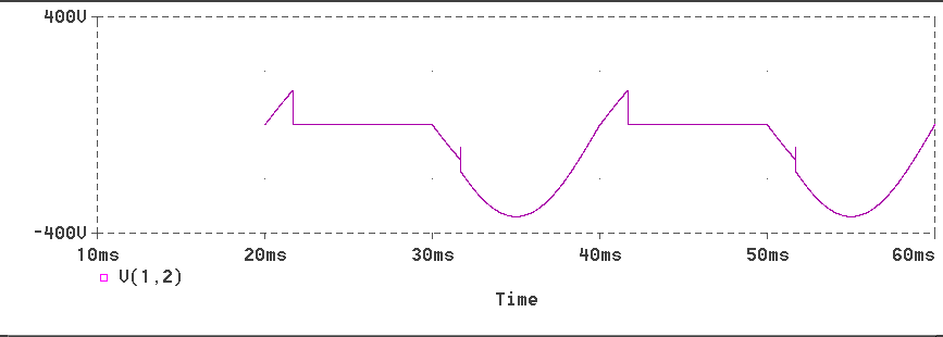
The voltage waveform across the load resistor

The voltage waveform across SCR1
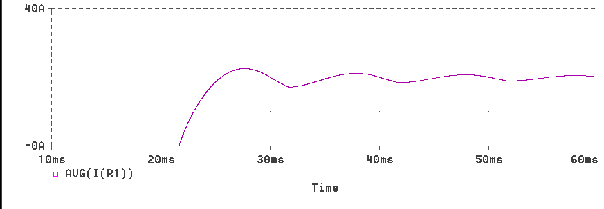
The average load current
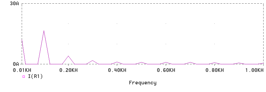
The Frequency spectrum of line current
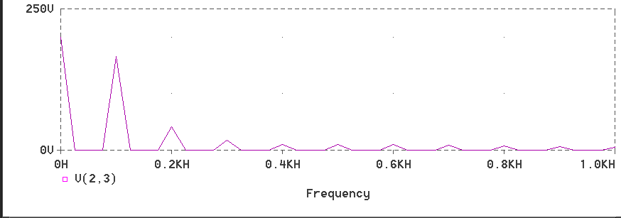
The Frequency spectrum of output voltage
You can either download or view the MathCad program file.
![]()
![]()
This page has described the operation of a fully-controlled
bridge rectifier circuit with a purely resistive load. The next page
describes how the circuit behaves when the load has a reactive and
a resistive component.