CIRCUIT DIAGRAM
SUMMARY
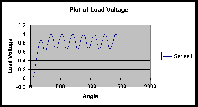
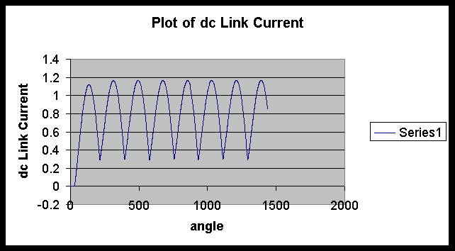
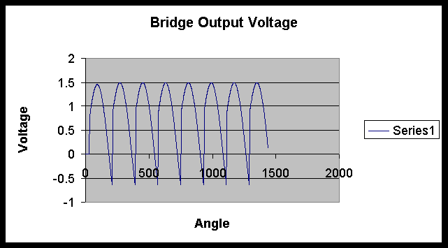
The operation of the circuit has been described in the earlier pages. One pair of SCRs conducts at a time, producing a bridge output voltage containing significant ripple content. Since the current through an inductor cannot change suddenly, the inductor in the dc link tries to maintain the current passing through it as a steady value, which in turn means that the ripple content of the current through it reduces. Nevertheless it does contain some ripple and this ripple in the inductor current causes some ripple in the capacitor voltage, whereas the current through the load can be more or less a steady value. The effectiveness of the filter circuit depends on the values of the inductor and the capacitor. The larger they are, the higher the reduction in the filter content is. Of particular interest is the comparison of the bridge output voltage and the capacitor voltage. The ripple in the capacitor voltage is almost out-of-phase with the ripple in the bridge output voltage. This aspect is important when the output voltage across the load resistor is to be controlled in closed loop.
The analysis of this circuit is slightly more complex. The differential equations that describe the operation of the circuit are presented below. Because of the filter capacitor, the current in the inductor can become discontinuous for a light load, even if the firing angle is not high. Hence the differential equations are described for the two cases separately.
DISCONTINUOUS CONDUCTION
When the current through the load is discontinuous, the
load current starts building up from zero value when one of the pair of
SCRs is triggered and it falls to zero before the next pair of SCRs is
triggered. Let the firing angle be a and
let the current through the inductor become 0 when wt = p
+ b, where b <
a. That is, there is current flow during a
< wt < (p + b)
SCRs S1 and S3 in conduction and during (p
+ a) < wt < (2p + b)
SCRs S2 and S4 in conduction. This means
that ther will no current flow during (p + b) <
wt < (p + a)
and b) < wt < a.
Let the supply voltage vs be E*Sin (q),
where q = wt. Let the voltage across the capacitor
be vC(q) and the current through
the inductor be iL. Then equations (1) and (3) are for the periods
when there would no current flow. When SCRs
S1 and S3 are in conduction, both the line current
and the load current have the same magntitude and polarity and equation
(2) applies. When SCRs S2 and S4 are in conduction,
the line current is the negative of the load current and equation (4) is
to be used. The current through the capacitor is the difference of
the dc link inductor current and the current through the load resistor,
as shown in equation (5).
CONTINUOUS CONDUCTION
For continuous conduction, it is sufficient if the equations are described for half-a-cycle only. In the other half-cycle, the only difference is in the source current waveform. Since the source current has half-wave symmetry, it is sufficient if it is described over half-a-cycle. Let the firing angle be a. Let the commutation overlap angle be d. Then it means the SCRs are triggered when q = a or when q = p + a, the process of commutation ends d radians later. Let the source current be is. Then during a < q < ( a + d ), the entire source voltage is applied across the source inductor, as shown in equation (6). During this period, the output voltage of the bridge is zero and the voltage across the inductor is then the voltage across the output capacitor. Since the voltage across the output capacitor tends to reverse the current through the inductor, equation (7) describes the current-voltage relationship in the inductor for this period. During ( a + d ) < q < (p + a) , the voltage across the source inductor and the dc link inductor is defined by equation (8). During this period, the line current and the load current have both the same magnitude and polarity, as shown by equation (9). Equation (10) defines the current-voltage relationship of the output capacitor. As shown in equation (10), capacitor current is the difference between the inductor current and the current through the load resistor.

SOLUTION
The solution of the equations for both the cases is carried
out using numerical technique.
In this section, the circuit is simulated. You have to key-in the firing angle in degrees, the ratio wLL/RL, the ratio wLs/RL and the average load current fraction. The ratios are specified for the nominal load conditions, assuming that the average output voltage is at its maximum and that the average load current is at its rated value. The setting for load current fraction allows for simulation under different load conditions. A setting of 1.0 means that the simulation is for rated load condition. When the setting is 0.25, it means that the average load current set is 25% of the rated load current. The applet below generates the waveforms for the parameters keyed-in.
The parameters for the next applet are the same as those
for the applet above. This applet prints out the statistics.
The pspice program used for simulation is as follows:
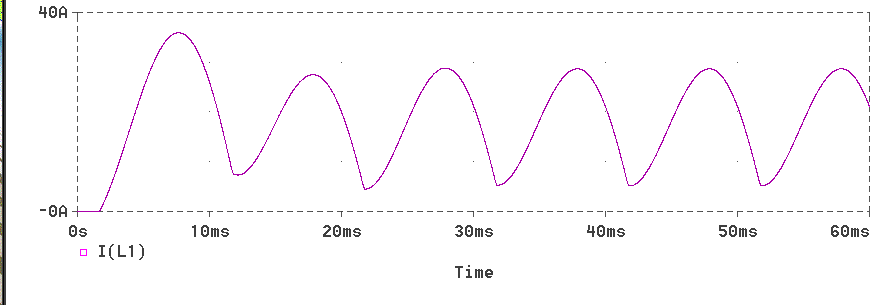
* Full-wave Bridge Rectifier with RL Load and source Inductance
VIN 9 0 SIN(0 340V 50Hz)
XT1 1 2 5 2 SCR
XT2 0 2 6 2 SCR
XT3 4 0 7 0 SCR
XT4 4 1 8 1 SCR
VP1 5 2 PULSE(0 10 1667U 1N 1N 100U 20M)
VP2 6 2 PULSE(0 10 11667U 1N 1N 100U 20M)
VP3 7 0 PULSE(0 10 1667U 1N 1N 100U 20M)
VP4 8 1 PULSE(0 10 11667U 1N 1N 100U 20M)
L1 2 3 31.8M
L2 1 9 1.6M
R1 3 4 10
C1 3 4 318.5u
R2 1 0 1MEG
R3 2 0 1MEG
R4 4 0 1MEG

* Subcircuit for SCR
.SUBCKT SCR 101 102 103 102
S1 101 105 106 102 SMOD
RG 103 104 50
VX 104 102 DC 0
VY 105 107 DC 0
DT 107 102 DMOD
RT 106 102 1
CT 106 102 10U
F1 102 106 POLY(2) VX VY 0 50 11
.MODEL SMOD VSWITCH(RON=0.0105 ROFF=10E+5 VON=0.5 VOFF=0)
.MODEL DMOD D((IS=2.2E-15 BV=1200 TT=0 CJO=0)
.ENDS SCR
.TRAN 10US 60.0MS 0.0MS 10US
.FOUR 50 V(2,4) I(VIN)
.PROBE
.OPTIONS(ABSTOL=1N RELTOL=.01 VNTOL=1MV)
.END
The results obtained are presented below.
The waveform of bridge output voltage

The waveform of bridge output current
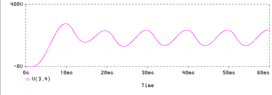
The waveform of voltage across the load
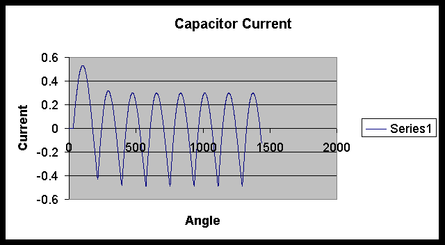
The waveform of filter capacitor current

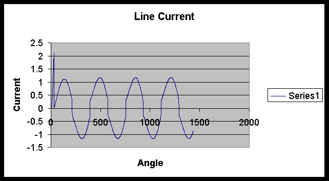
The waveform of line current
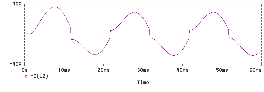
The waveform of dc link inductor voltage

// Simulation of a single-phase fully-controlled bridge
// rectifier circuit.
// This program produces the transient response, the periodic
// response. Commuation overlap angle is also computed.
// Calculations normalized.  The average voltage that would
// occur for diode-bridge rectifier with a resistive load is
// taken to be unity.  The average current through the load
// resistor with a pure resistive load on the diode bridge
// rectifier is taken as the unity current.  The parameters to
// be fed are just three: the ratio of load inductive reactance
// to the load resistance, wL1/R , the ratio of source reactance
// to the load resistance to load resistance wL2/R and the firing
// angle in degrees.


#include <math.h>
#include<stdlib.h>
#include<stdio.h>
#include<string.h>
#include<iostream.h>

void kreateRespFile(void);
void tranResponse(void);
void OneCycle(void);
void computeOneStep(void);
void produceEntries(void);


const double pi=3.1415926;
const double deg_rad=pi/180.0;
const double step=pi/720.0;

double L1,L2,alpha,fang,elapseAng,cycleAng,tote_knt;
double cur_load,cur_line,outVolt,vSource,vInput,capVolt;
double OverLapangle,Cap,capCur,dcLinkCur,Res;
int commute,toggle,yes_Entry,modeSw;
FILE *fnew;
char *tstr,*p;


int main(void)
{
 float  ka1,kb2,kc3,kd4,ke5;
 printf(" \n");
 printf("     Load Time Constant in radians = ");
 scanf("%f",&ka1);
 L1=(double)ka1;
 if (L1<0.05) L1=0.05;
 printf(" \n");
 printf("     Line Reactance Time Constant in radians = ");
 scanf("%f",&kb2);
 L2=(double)kb2;
 printf(" \n");
 printf("   Cap. Filter Time Constant in radians   = ");
 scanf("%f",&kc3);
 Cap=(double)kc3;
 if (Cap<0.1) Cap=0.1;
 if (Cap>10.0) Cap=10.0;
 printf(" \n");
 printf("   Load Resistance in p.u.   = ");
 scanf("%f",&ke5);
 Res=(double)ke5;
 if (Res<0.1) Res=0.1;
 if (Res>10.0) Res=10.0;
 printf(" \n");
 printf("     Firing angle in degrees = ");
 scanf("%f",&kd4);
 alpha=(double)kd4;
 fang=alpha*deg_rad;
 alpha=0.0;
 printf("  \n");

 // Initialise though not necessary for global variables

 elapseAng=0.0 ;  cycleAng=0.0;  capCur=0.0;  capVolt=0.0;
 cur_load=0.0;  cur_line=0.0;  outVolt=0.0;  tote_knt=0.0;
 OverLapangle=0.0;  commute=0;  yes_Entry=0; dcLinkCur=0.0;
 cur_load=0.0;


 // Create a file for entering transient response
 fnew=fopen("tran_v3.csv","w+r");
 tranResponse();
 fclose(fnew);
 return 0;
}

void kreateRespFile(void)
{
 int n1,n2;
 tstr="Angle,InputV,VoutBr,dcLinkCur,LineCur,IndVolt,LoadVolt,capCur";
 p=strtok(tstr,",");
 fprintf(fnew,p); fprintf(fnew,",");
 n2=8;
 for (n1=0;n1<(n2-1);n1++)
        {
         p=strtok(NULL,",");
         if (n1!=(n2-2))
                {
                 fprintf(fnew,p); fprintf(fnew,",");
                }
         else
                {
                 fprintf(fnew,p); fprintf(fnew,"\n");
                }
        }
}

void tranResponse(void)
{
 double d1;
 int NumCycles,count;
 d1=(6.0*(L1+L2+Cap))/(2.0*pi)+0.5;
 NumCycles=(int)d1 + 1;
 kreateRespFile();
 modeSw=1;
 for (count=0;count<=NumCycles;count++)
        OneCycle();
}


void OneCycle(void)
{
 int knt;
 double dknt;
 dknt=0.0;


 for (knt=0;knt<1440;knt++)
        {
         cycleAng=dknt*step;
         vInput=pi/2.0*sin(cycleAng);
         if ((cycleAng<fang) || (cycleAng>(fang+pi)))
                {
                 if (cycleAng<fang) vSource=pi/2.0*sin(cycleAng+pi);
                 else vSource=pi/2.0*sin(cycleAng-pi);
                 toggle=0;
                }
         else
                {
                 vSource=pi/2.0*sin(cycleAng);
                 toggle=1;
                }
         if (modeSw!=toggle)
                {

                 commute=1;
                 if (L2<0.0005) commute=0;
                 modeSw=toggle;
                }
         computeOneStep();
         dknt+=1.0;
        }
}

void computeOneStep(void)
{
 double dLoadI,dLineI,doutV;

 switch (commute)
        {
         case 0:
          dLoadI=(vSource-dcLinkCur)/(L1+L2)*step;
          doutV=(dcLinkCur-capVolt/Res)*step/Cap;
          dcLinkCur=dcLinkCur+dLoadI;
          capVolt=capVolt+doutV;
          if (capVolt<0.0) capVolt=0.0;
          if (dcLinkCur<0.00001) dcLinkCur=0.0;
          if (toggle==0) cur_line=-dcLinkCur;
          else cur_line=dcLinkCur;
          outVolt=cur_load+(vSource-cur_load)*L1/(L1+L2);
          cur_load=capVolt/Res;
          capCur=dcLinkCur-cur_load;
         break;

         case 1:
          dLoadI=(0.0-cur_load)/L1*step;
          doutV=(dcLinkCur-capVolt/Res)*step/Cap;
          dcLinkCur=dcLinkCur+dLoadI;
          capVolt=capVolt+doutV;
          if (capVolt<0.0) capVolt=0.0;
          if (dcLinkCur<0.00001) dcLinkCur=0.0;
          dLineI=vInput/L2*step;
          cur_line=cur_line+dLineI;
          if (toggle==1)
                {
                 if (cur_line>dcLinkCur) commute=0;
                }
          if (toggle==0)
                {
                 if ((cur_line+dcLinkCur)<0.0) commute=0;
                }
          if (dcLinkCur<0.00001) outVolt=capVolt;
          else outVolt=0.0;
          cur_load=capVolt/Res;
          capCur=dcLinkCur-cur_load;
         break;
        }
 tote_knt+=1.0;
 elapseAng=tote_knt*step;
 alpha=tote_knt/4.0;
 yes_Entry+=1;
 if (yes_Entry==4) produceEntries();
 if (yes_Entry==4) yes_Entry=0;
}

void produceEntries(void)
{
 double negate;
 gcvt(alpha,5,p);
 fprintf(fnew,p);
 fprintf(fnew,",");
 gcvt(vInput,5,p);
 fprintf(fnew,p);
 fprintf(fnew,",");
 gcvt(outVolt,5,p);
 fprintf(fnew,p);
 fprintf(fnew,",");
 gcvt(dcLinkCur,5,p);
 fprintf(fnew,p);
 fprintf(fnew,",");
 gcvt(cur_line,5,p);
 fprintf(fnew,p);
 fprintf(fnew,",");
 if (toggle==0) negate = 1.0; else negate=-1.0;
 gcvt(vInput-negate*outVolt,5,p);
 fprintf(fnew,p);
 fprintf(fnew,",");
 gcvt(capVolt,5,p);
 fprintf(fnew,p);
 fprintf(fnew,",");
 gcvt(capCur,5,p);
 fprintf(fnew,p);
 fprintf(fnew,"\n");
}
The above program can be downloaded by clicking on the image
displayed below.

This page has described the effect of adding a filter capacitor. It can also be seen that no attempt is made to obtain the periodic response by determining the coefficients, since it is easier to use the numerical technique to obtain the solution. The next page describes an application of this circuit.