The circuit diagram of a battery charger is shown above. The ac source and the inductance in series with it can represent a transformer and its leakage inductance as viewed from its secondary. In a battery charger circuit, the current supplied by the source is usually discontinuous and the load across the battery is usually very light.
The behaviour of a fully-controlled bridge circuit has been described in the previous pages. This page describes how the battery-charger can be controlled in closed-loop. Traditionally systems use controllers such as a PI controller or a PDF controller for feedback control. But a battery has a very large time constant and control of a system with a large time constant is not easy. Hence the controller described in this page is a rule-based controller. It can be implemented either with traditional logic gates, counters and ADCs or by using a micro-controller and some more ICs to complement its operation.
The battery is modeled mainly as a very large capacitor and a series resistor RB. The capacitance used in the model is not as large as the value that can represent the stored AH capacity of the battery, since that would lead to a very large period for simulation. The capacitance used is large enough to make the behaviour of the system similar to that of a real battery-charger, but small enough to get the simulation performed in a reasonable time.
Firstly, a method by which the phase-angle can be controlled
is explained and then the rule-based controller is described. A synchronizing
voltage, usually the output from a secondary winding of a transformer with
its primary connected to the mains supply, is fed to a zero-crossing detector.
In the scheme described here, two logic signals are developed; logic
signal A is set to high level when the synchronizing voltage crosses zero,
becomes positive and stays positive, and logic signal B is set to high
level when the synchronizing voltage crosses zero, becomes negative and
stays negative. If the synchronizing signal is described to be E*Sin
(q), it would be preferable if A is at 1 from
q = 5o to q
= 175o and B is at 1 from q
= 185o to q = 355o .
Then a logic NOR signal, A NOR B , can be obtained. The NOR
signal can be used to reset a ramp generator when the synchronizing signal
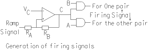
crosses zero in either direction. The ramp output can then be compared
with a control voltage VC and the output C of comparator can
be ANDed with either A or B. The logic signal, A AND C, can be used
to generate a firing signal for SCRs S1 and S3.
It can be seen that these SCRs are triggered when the source voltage Vs
is positive, provided that the synchronizing signal is in phase with the
mains supply voltage. The logic signal, B AND C, can be used to generate
a firing signal for SCRs S2 and S4. It can
be seen that these SCRs are triggered when the source voltage Vs
is negative.
The scheme outlined can be implemented in different ways.
One of the methods that can be followed is described next.
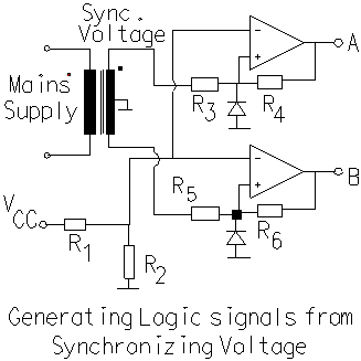
From the mains supply, a synchronizing signal can be obtained. If a single-polarity supply is to be used, CMOS opamps, suitable for operation with a single power supply, can be used. The resistors have to be chosen to suit the requirements. For example, let the peak of synchronizing voltage be 10 V. If the ramp is to start at 5o, then the magnitude of ramp signal would be 10 * Sin (5o), which is 0.871 V. If VCC is 12 V, then R1 and R2 can be selected such that the voltage across R2 is 0.871 V. The values of R3 and R4 are selected that the ratio (R3/R4) is very small, of the order of about 0.01.
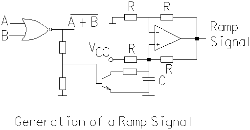
The circuit to generate the ramp signal is shown above.
Whenever the signal, A NOR B, is at 1, the transistor is switched ON and
it discharges the capacitor. When the NOR signal becomes zero, the
boot-strap integrator generates a ramp signal at its output.
If the ramp signal is be called y(t), then
where t starts from zero from the instant the transistor stops conducting. The values of R and C should be chosen such that when the synchronizing voltage varies from 10 * Sin (5o) to 10 * Sin (175o), the ramp signal varies from 0 V to about 10 V. The time corresponding to 170o depends on the frequency. At 50 Hz, the corresponding time period is 9.444 ms and it is 7.87 ms. When the ramp signal varies in this manner, the control voltage can be varied from 0 V to 10 V to vary the firing angle. For the boot-strap integrator also, a CMOS opamp can be used . It would be preferable to use a CMOS opamp as the comparator too. From the comparator output and the logic signals A and B, the signals that can be used to generate firing pulse for the SCRs is described next.
A firing signal for an SCR can be generated in several ways. For high power SCRs, the best technique is to use a pulse transformer with a ferrite core. But in an application such as the battery-charger with a single-phase fully-controlled bridge rectifier circuit, the rating of the SCRs is not likely to be in the range of hundreds of amperes and it may be preferable to use an opto-coupler with light-activated SCR detector.

One opto-coupled light-activated triggering IC is required for each SCR. It would be preferable to connect a resistor between the gate and the cathode of light-activated SCR. Its value can be in the region of several kilo-ohms and it depends on the IC used. The light-activated SCR in turn triggers the main SCR as shown below. For the SCRs in the bridge rectifier circuit also, it would be preferable to connect a resistor between the gate and the cathode, and its value can be about 500 W. In addition, it would be necessary to connect a snubber circuit from the anode to cathode of each SCR. The values of components to be used for the snubber circuit can be normally obtained from the datasheet of the SCR. It should also be remembered that the blocking voltage of the light-activated SCR should be the same as that of the main SCR.
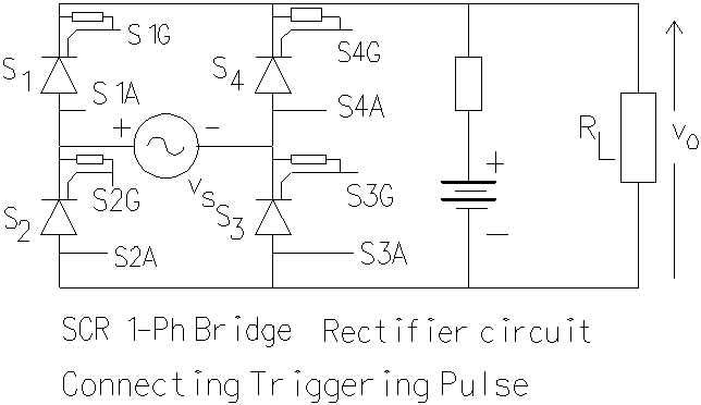
The source that drives the bridge circuit is usually the secondary of a transformer. The leakage inductance of the transformer as viewed from the secondary terminals acts as the source inductance for the circuit. With a light load, the bridge output tends to be discontinuous. The next section describes how the circuit operates.
The equations are normalized. The nominal voltage of the battery is taken to be 1 p.u and the nominal rms current of the secondary of the transformer is taken to be 1 p.u. For example, let the nominal voltage of the battery bank be 72 V. Let the rms secondary voltage be 100 V and its rated rms current be 10 A. Then the peak secondary voltage equals (1.414*100/72), that is 1.964 p.u. If the drop in terminal voltage of the battery bank when it delivers 10 A is 1 V, then its source impedance is set to be 1.414/72, that is 0.0196 p.u.
The load current drawn by the load resistor should be relatively low, less than 0.25 p.u. That is, 0.3 p.u corresponds to 4.24 A the corresponding load resistance is 72/4.24, that is 17 W.
The simulation routine is explained below. All setting are in per unit notation.
Initializing routine:
Set the
value of peak secondary voltage
Set the
value of fractional load
Set the
source inductance.
Set the
peak battery current
Set the
maximum average battery current
Set the
initial battery voltage(internally set)
Set the
time constant of the battery(set to 300 radians internally)
Set the
source resistance of the battery
Set the
firing angle to 175o (internal setting)
Reset to
zero the battery current. peak charging current.
Reset to
zero the rms secondary current. average battery charging current.
Go to pre-amble
routine
Pre-amble routine:
Print the
battery voltage
Print the
average battery voltage
Print the
peak charging current
Print the
rms secondary current
Set
the rule-based controller as follows:
if (average Battery Current =(1.1*maximum average battery
Current))
increase the firing angle by 1o
else
{
if ((batteryVolt<=1.1) and (average Battery Current <maximum
average battery Current))
decrease the firing angle by 1o
if ((batteryVolt<=1.1) and (average Battery Current =maximum
average battery Current))
do no change the firing angle
if ((batteryVolt1.1) and (batteryVolt<=1.15)) do no change
the firing angle
if (batteryVolt1.15) increase the firing angle by 1o
}
if (peakBtyCurpeakCurSet) increase the firing angle by 2o
Reset
to zero peak charging current, average battery current and rms secondary
Current.
Go to One-Output-Cycle
routine.
One-Output-cycle routine:
angle=0;
while
( angle =0 and angle <180 )
{
compute increments in battery voltage and source current
compute increments to rms secondary current, average battery charging current
set the peak battery charging current appropriately
increment angle by step size
}
The applet below demonstrates how a rule-based battery charger would function.
Next page describes how a dc motor can be controlled in closed-loop.