
i. A slight reduction in output voltage,
ii. A notch in the supply voltage to the circuit during
commutation overlap.
When the source has inductance, other loads connected to this source along with the controlled rectifier are supplied voltages with notches in them and some of these loads can be sensitive to these notches and they may operate improperly. Hence in order to reduce the magnitude of notches, it is mandatory in some countries for the rectifier to be provided with an inductance in series with each of its three-phase input lines. If these inductors are much larger than the source inductance, the notch voltages are absorbed by these inductances and the other loads connected to the same 3-phase source are not supplied with distorted voltages. The internal inductances connected in series with the source are sometimes referred to as 4% inductances. If the inductor is such that the voltage drop across it is about 4% of the phase voltage at rated current, it is normally sufficient to reduce the notches at the source terminals to an acceptable level.
When there is an inductor in series with each input line, it is necessary to find out its effect. We need to find out:
a. The reduction in output voltage.
b. The duration of commutation overlap.
c. The relationship between the firing angle and the
commutation overlap.
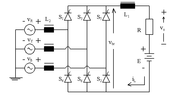
REDUCTION IN OUTPUT VOLTAGE
Calculations by hand are carried out assuming that the
dc link current remains steady without any ripple. The source voltages
at its terminals and the output voltage appear as shown below, assuming
that the inductances belong to the source.
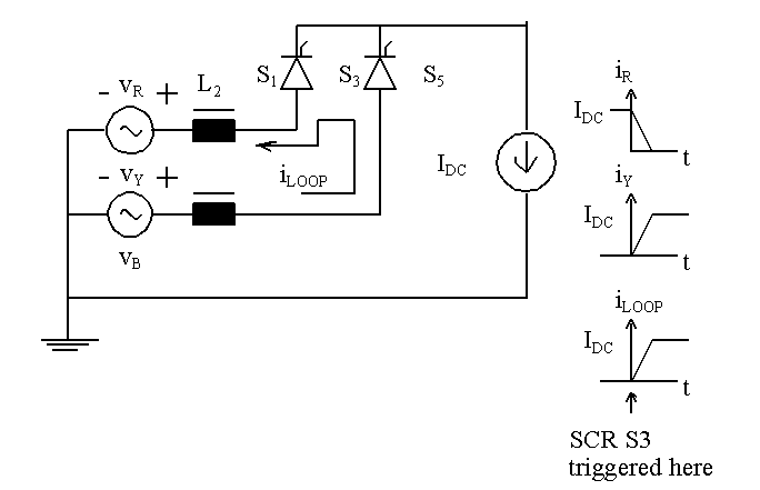
It is seen that there are six notches in one input cycle. The reduction in average output voltage can be found out as follows. Let SCR S1 be in conduction and let S3 be triggered. Let the current through the dc link be IDC. Then current through Y-phase has to rise from zero to IDC, whereas current through R-phase has to fall from - IDC to zero. On the other hand, loop current iLOOP marked in the sketch below has to rise from zero to IDC. This means that during commutation current through Y-phase would rise from zero to IDC and the volt-second area the output misses out is L2IDC, that absorbed by the inductor in the Y-phase.
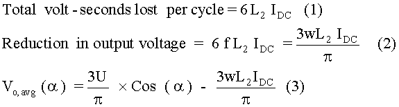
From the volt-seconds lost per commutation, we can find the total volt-seconds lost in one input cycle. Since there are six commutations per cycle, the total volt-seconds lost per cycle is expressed as shown by equation (1). Dividing this area by the time corresponding to one cycle, we get the average voltage reduction in output. The time corresponding to one input cycle is 1/f, where f is the line frequency. Then the average reduction in output voltage is obtained as shown in equation (2). In equation (2), we make use of the relation that the angular frequency, w = 2pf. It is to be noted that commutation overlap occurs only when there is continuous conduction through the load and the average output voltage is expressed by equation (3). In equation (3), U is the peak line-to-line voltage and a is the firing angle.
COMMUTATION OVERLAP ANGLE
The commutation of commutation overlap depends on:
a. the firing angle,
b. the dc link current and
c. the source inductance or the inductance in series
with each phase.
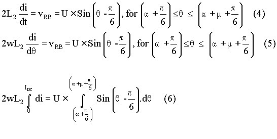
To find out the commutation overlap, it is sufficient
to analyse one commutation. Let SCR S5 be in conduction and
let SCR S1 be triggered at a firing angle of a.
As seen earlier, the loop current iLOOP builds up from zero
to IDC. This means that the current in the inductance in R-phase
builds up to IDC, whereas it decreases to zero in the inductance
in the B-phase. Let the commutation last for an angle m.
Then during commutation, the voltage across the source inductance is expressed
as shown in equation (4). In equation (4), the loop current is denoted
as ‘i’. Since q = wt, the equation for commutation
overlap can be represented as shown in equation (5). During this interval,
the loop current changes from zero to IDC. Hence equation (6)
defines how current in R phase changes.
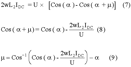
The solution of equation (6) is presented in equation (7). Equation (7) can be re-arranged and presented as shown in equation (8). Solving for m, we obtain equation (9).
It is seen that overlap angle m increases
a. as the firing angle moves closer to either 0o
or 180o ,
b. as the dc link current becomes larger, and
c. as the link inductance gets larger.
The above equation has been obtained based on the assumption that the dc link current remains steady, which happens only when the dc link inductance is relatively large. In practice, it is not true and hence the above equation yields only an approximate result.
The rest of mathematical analysis follows the familiar route. The items of interest are:
a. RMS output voltage of bridge circuit,
b. Average output voltage of bridge circuit,
c. Ripple Factor of output voltage of the bridge,
d. RMS output voltage/voltage across load resistor,
e. Average output voltage (across load resistor),
f. Ripple factor of output voltage (across load resistor),
g. RMS line current,
h. RMS value of fundamental component in line current,
i. THD in line current,
j. Displacement power factor,
k. Apparent power factor and
l. Harmonic analysis.
In order to simulate it is necessary to have an expression
for line current and load current. Let us consider one output cycle, starting
from the instant SCR S1 is triggered till SCR S2
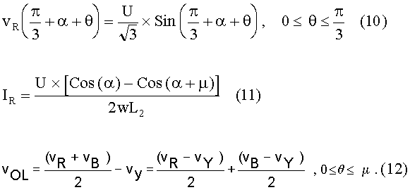
is triggered. During this period, the R-phase is defined as shown in equation
(10). When SCR S1 is triggered, we have commutation overlap
till the load current is transferred from SCR S5 to SCR S1
and let the commutation overlap angle be m.
During commutation overlap, the current through SCR S1 rises
from zero to load current. At the end of commutation overlap, line current
is obtained from the expression in equation (11). During the period of
commuation overlap, the voltage source that is seen by the dc link circuit
is described as shown in equation (12), where vOL represents
the source during overlap period.
On simplifying equation (12), we get equation (13). During
this period, the source appears to have a source inductance equalling 1.5L2
. We get this value because the path through SCR S6 contains
L2 whereas the path through both S1 and S5
appears to have an equivalent inductance of value equal to 0.5L2.
The current through the load at the instant when SCR S1 is triggered
can be expressed as shown in equation (14).. The values of Z and f
in equation (14) are expressed in equation (15).
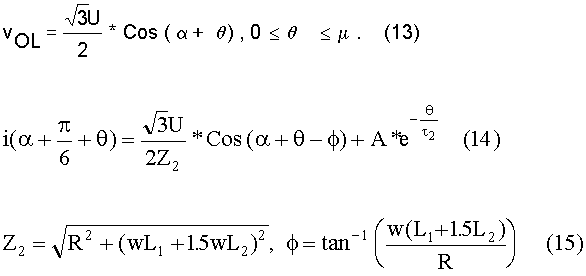
The constant A in equation (14) is to be evaluated and t2 = tan (f). At the end of commutation, this current would be equal to the line current. Hence we obtain equation (16). The terms used in equation (17) are defined in equation (18).
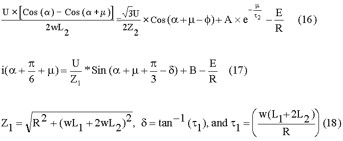
Equation (16) is the first of the three equations we
need in order to obtain a solution and this equation equates the line current
to the load current at the end of commutation. Equation (17) expresses
the load current at the end of commutation, using another constant B and
B is also to be evaluated. Another equation can be formed as shown in equation
(19), which equates the line current at the end of commuation to the load
current. Unlike equation (16), equation (19) makes use of constant
B. Equations (16) and (19) are two of the three equations required
to solve for A, B and d. The third equation
is obtained as follows. The load current at the instant when q
= p /3 can be computed in two ways, one from
equation (16) and the other from equation (19) and these two expressions
can be equated to yield equation (20).
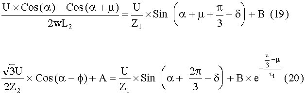
From these three equations, the three unknowns, A, B
and m, can be obtained. These equations have
been used in the program written for simulation.
Three applets are presented in this section. The first applet animates the circuit. The only purpose is to illustrate the sequence of operation of this circuit. It does not take in any parameter. To run it, click on the RUN button. The SINGLE STEP button allows the user to step through, the PAUSE button allows the user to stop the program and the RESET button allows the user to view the simulation once more. To view the simulation once more, click on the RESET button and then click on the RUN button. During the simulation, the user can ask the program to pause for a while, then step through for a while and allow it to run through to the end of its cycle.
The second applet takes in these parameters:
a. the firing angle in degrees,
b. the ratio of load reactance to load resistance (load reactance evaluated at line frequency),
c. the ratio of source reactance to load resistance(preferably below 0.1 p.u), and
d. the value of dc link source.
The program allows you to view either the waveforms or the statistics. The values of load and line reactance are to be entered in per unit. For example, if the line reactance is entered as 0.05 p.u., rated load current would cause a drop of 4% of phase voltage across the line reactance.
An example is presented now to explain how the per unit values can be set. Let a 3 phase, 415 V, 50 Hz source supply power to the converter. Then the maximum average voltage that can be obtained is obtained as shown below. Let the nominal rated dc link current be 100 A. Then the nominal load resistance or the base impedance for the system is computed as shown below. It is also shown how the line reactance can be obtained, if its value in p.u. is known. Given that the current through the load is free of ripple, the rated RMS line current is obtained as illustrated below. From the total rms line current, inclusive of both the fundamental component and the harmonic components, the fundamental rms component is obtained as illustrated below.
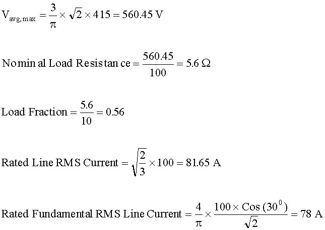
Given that the line inductance is 1 mH, its p.u. value
is obtained as shown below.
Given that the dc link inductance is 10 mH, its p.u.
value is computed as illustrated below.
Usually the line inductance is called as the 4% reactor,
implying that when the line current is at its rated value, the rms value
of the fundamental component of voltage across the line reactor is 4% of
the phase voltage. For example, if the rms phase voltage is 240 V,
the drop across 4% reactor at rated current would be 9.6 V. When
the line voltage is 415 V, the phase voltage is calculated as shown below.
The drop across the line inductor can now be stated as a
fraction of the phase voltage as given below.
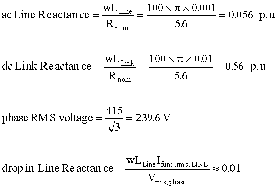
This means that if the drop across the line inductor is
to be 4% of phase voltage, the inductance should be 0.4 mH and not 1 mH.
The third applet takes in these parameters:
a. the ratio of load reactance to load resistance (load
reactance evaluated at line frequency),
b. the ratio of source reactance to load resistance(preferably
below 0.1 p.u), and
c. the value of dc link source.
Within the program the firing angle is varied and the
plots of rms bridge output voltage, the average bridge output voltage,
its RF, the rms line current, the fundamental rms component of line current,
the THD in line current, the average output current, its RF and the overlap
angle as a function of firing angle are displayed. The value of dc
source in the dc link is assigned to be zero in this applet.
MATHCAD SIMULATION
The MathCad file can be downloaded
by clicking on the image below.
![]()
A C-program called, ss_resp.cpp, can be downloaded by
clicking on the image below. It can be compiled as a C program and
executed.
![]()
The program was run with the following values:
Time constant of the Link inductor in radians: 1.00
Time constant of the Source Inductance in radians : 0.03
Firing Angle = 30o.
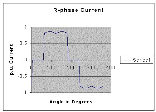
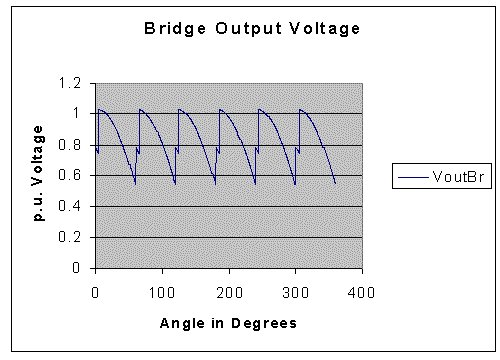
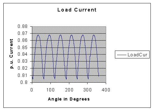
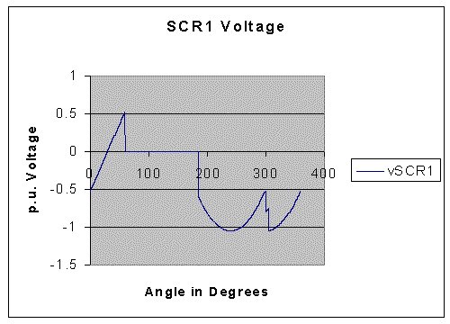
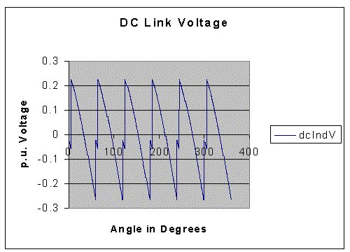
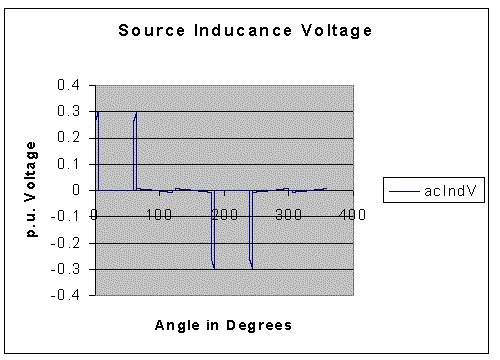
The results obtained are presented below.
Another C-program called, harm3ph.cpp, can be downloaded by clicking on the image below. It can be compiled as a C program and executed.
![]()
The results obtained for the same parameters are presented
below.
| harmNo | LoadCur | OutVolt | harmNo | LineCur |
| 0 | 1.6874 | 1.6872 | 1 | 0.93105 |
| 2 | 2.69E-08 | 1.16E-08 | 3 | 2.31E-08 |
| 4 | 2.75E-08 | 2.94E-08 | 5 | 0.19975 |
| 6 | 0.029517 | 0.1743 | 7 | 0.1142 |
| 8 | 2.85E-08 | 2.82E-08 | 9 | 1.85E-08 |
| 10 | 2.85E-08 | 3.00E-08 | 11 | 0.080921 |
| 12 | 0.00639 | 0.074642 | 13 | 0.061509 |
| 14 | 2.87E-08 | 2.90E-08 | 15 | 1.82E-08 |
| 16 | 2.86E-08 | 2.97E-08 | 17 | 0.048484 |
| 18 | 0.0023099 | 0.040382 | 19 | 0.040233 |
| 20 | 2.87E-08 | 2.91E-08 | 21 | 1.84E-08 |
| 22 | 2.87E-08 | 2.94E-08 | 23 | 0.032741 |
| 24 | 0.0009234 | 0.021504 | 25 | 0.02832 |
| LoadIAvg | 0.84371 | |||
| LoadIRMS | 0.84398 | |||
| RFCur | 0.021433 | |||
| VoAvg | 0.84362 | |||
| VoRMS | 0.85546 | |||
| RFVolt | 0.14184 | |||
| ILineAvg | 0.56248 | |||
| ILineRMS | 0.68481 | |||
| THD | 0.684811 | |||
| OverLapAngle | 0.085085 |
This page has explained how source inductance leads to commutation overlap and how it affects the output voltage. Next page how a DC power supply can be built using the 3-phase fully-controlled bridge rectifier.