The simulation program is based on the pseudo-code displayed below.
Start block:
Set the values of load reactance,
line reactance, capacitor, load fraction.
Set the desired output voltage,
PI controller parameters
Set the current firing angle
to be 120o.
Set base reference angle to 60o.
Set Commute = 0. (
Indicates no commutation overlap exists at start. )
Go to Loop Routine.
Set theta to zero.
Loop Routine
Call Compute routine.
Increment theta.
If {(theta + base reference angle)
= (next firing angle) }
[
current
firing angle = next firing angle.
base reference
angle = next firing angle - 60o.
Set Commute
= 1 . ( Indicates next SCR is triggered)
]
Execute Loop Routine
Compute Routine:
If (Commute == 0)
[
compute
next value of link inductor current.
]
else
[
compute
next value of triggered SCR current.
compute
next value of link inductor current.
if
(SCR current link inductor current) Reset Commute to 0.
]
Compute next value of capacitor
voltage.
Compute next value of PI controller's
output.
Compute next firing angle.
The equations used in the Compute Routine
are obtained as follows.
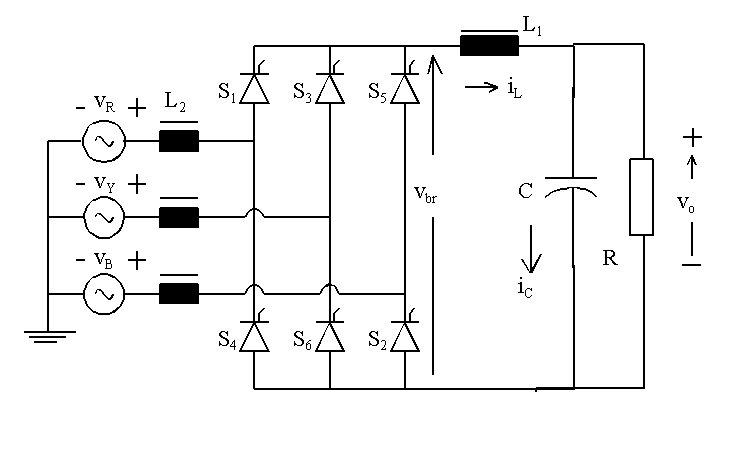
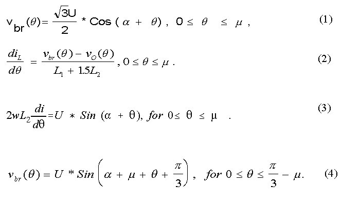
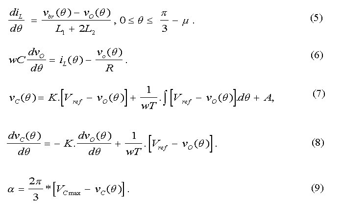
When there is commutation overlap, the output voltage
behind the source inductance is expressed by equation (1). In equation
(1), m is the
overlap angle and U is the amplitude of line voltage. If the output
voltage be vo(q) during this period,
the differential equation for the current through the dc link inductance
is presented as equation (2). During commutation
overlap, the current in the SCR just triggered on is described by equation
(3). The commutation overlap ends when
the current through this SCR equals the dc link inductor current.
When there is no overlap, the bridge output voltage is described by equation
(4).
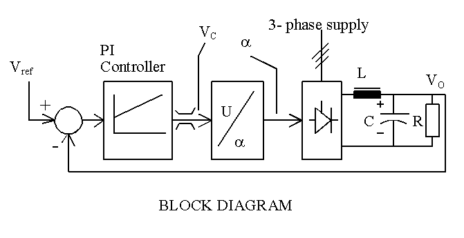
The differential equation that describes the dc link inductor current is then described by equation (5). The differential equation for the capacitor voltage is easily obtained and it is expressed as equation (6). Next the equations relating to closed-loop control are described. Let the output of PI controller be vC(q) and it is expressed by equation (7). In equation (7), A is a constant to be evaluated, K is the proportional gain of the controller and T is its time constant. The above equation is represented as equation (8) , which is more convenient for use in simulation. In equation (8), Vref is the desired output voltage. The output of the controller is normally checked to ensure that it is within the set limits. From the output of the controller, the firing angle, a can be obtained. The maximum output voltage of the controller should correspond to zero degree firing angle and the minimum to 120o firing angle. Hence we get the following equation for firing angle. This means that the range for vC(q) is from 0 to VCmax.
The simulation program uses the above equations and displays
the results in a graphical format.
The applet below can be run with the default parameters. To set any parameter, click on the arrow pointing downwards beside the Peak Source Voltage, a menu would appear. The default value of the parameter highlighted appears in the textfield for Set Value. To change the parameter, select the parameter and then click within the editable textfield for Set Value. In order to change this parameter, you must click on Set Value button. You can set the desired response to be one of three responses.
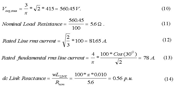
An example is presented now to explain how the per unit
values can be set. Let a 3 phase, 415 V, 50 Hz source supply power
to the converter. Then the maximum average voltage that can be obtained
is presented in equation (10). Let the nominal
rated dc link current be 100 A. Then the nominal load resistance
or the base impedance for the system is assigned as shown by equation (11).
Given that the current through the load is free of ripple,
the rms line current is obtained according to equation (12) and this value
includes both the fundamental component and the harmonic components.
The fundamental rms component is obtained as illustrated by equation (13).
Given that the dc link inductance is 10 mH, its p.u. value is obtained
as shown by equation (14).
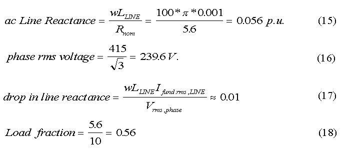
Given that the line inductance is 1 mH, its p.u. value
is obtained as shown by equation (16). Usually the line inductance is called
as the 4% reactor, implying that when the line current is at its rated
value, the rms value of the fundamental component of voltage across the
line reactor is 4% of the phase voltage. For example, if the rms
phase voltage is 240 V, the drop across 4% reactor at rated current would
be 9.6 V. When the line voltage is 415 V, the phase voltage is obtained
as shown by equation (16). The drop across the line inductor can now be
stated as a fraction of the phase voltage as given by equation (17).
This means that if the drop across the line inductor is to
be 4% of phase voltage, the inductance should be 0.4 mH and not 1 mH.
It is possible to set the load resistance to a value other
than its nominal value. The nominal value of load resistance is 5.6
W. If the load resistance is to be 10
W, then set Load Fraction as shown
by equation (18).